Capacitor and method for fabricating the same

a technology of capacitors and capacitors, applied in the direction of capacitors, fixed capacitor details, electrical equipment, etc., can solve the problems of difficult to secure the desirable capacitance of capacitors for device operation, thin film stress, and difficult to form capacitors, so as to reduce the stress of thin film

Inactive Publication Date: 2009-11-05
SK HYNIX INC
View PDF2 Cites 32 Cited by
  • Summary
  • Abstract
  • Description
  • Claims
  • Application Information

AI Technical Summary

Benefits of technology

[0006]Embodiments of the present invention are directed to providing a capacitor, which can reduce a thin film stress between a dielectric layer and an electrode, and a method for fabricating the capacitor.

Problems solved by technology

Thus, it is difficult to secure a desirable capacitance of a capacitor demanded for device operation.
In particular, it has become difficult to form a capacitor which embodies an appropriate capacitance needed to operate a giga-byte class dynamic random access memory (DRAM) device on a semiconductor substrate.
However, using a multi-component dielectric layer may cause a thin film stress due to a lattice mismatch and deteriorate capacitance and leakage current due to a low-k interface layer formation.

Method used


Image

  • Capacitor and method for fabricating the same
  • Capacitor and method for fabricating the same
  • Capacitor and method for fabricating the same

Examples


Embodiment Construction

[0025]Other objects and advantages of the present invention can be understood by the following description, and become apparent with reference to the embodiments of the present invention.

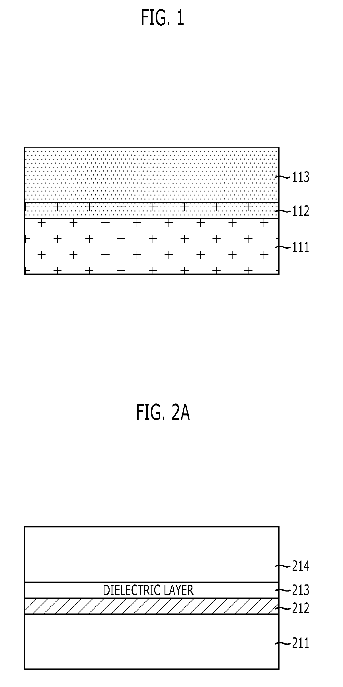
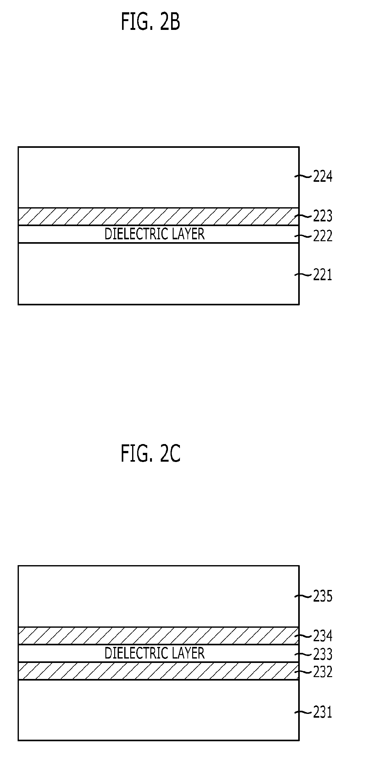
[0026]In the figures, the dimensions of layers and regions may be exaggerated for clear illustration. Also, when a layer (or film) is referred to as being ‘on’ another layer or substrate, it includes a meaning that the layer is directly on the other layer or substrate, or that intervening layers may also be present. Furthermore, when a layer is referred to as being ‘under’ another layer, it includes a meaning that the layer is directly under, or that one or more intervening layers may also be present. In addition, when a layer is referred to as being ‘between’ two layers, it includes a meaning that the layer be the only layer between the two layers, or that one or more intervening layers may also be present.

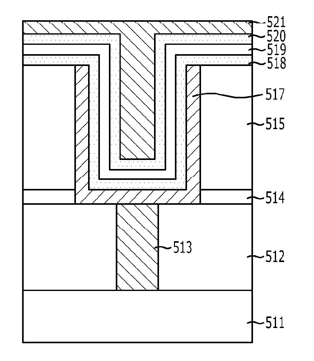
[0027]Embodiments of the present invention relate to a capacitor and a method for fabricating...


PUM

PropertyMeasurementUnit
temperatureaaaaaaaaaa

Abstract

A capacitor includes a first electrode, a dielectric layer, and a second electrode. The capacitor also includes a buffer layer formed over at least one of an interface between the first electrode and the dielectric layer and an interface between the dielectric layer and the second electrode, wherein the buffer layer includes a compound of a metal element from electrode materials of one of the first and second electrodes and a metal element from materials included in the dielectric layer.

Description

CROSS-REFERENCE TO RELATED APPLICATIONS[0001]The present invention claims priorities of Korean patent application number 10-2008-0040923, filed on Apr. 30, 2008, and Korean patent application number 10-2008-0137314, filed on Dec. 30, 2008, the disclosures of which are incorporated by reference in their entireties.BACKGROUND OF THE INVENTION[0002]The present invention relates to a method for fabricating a semiconductor device, and more particularly, to a capacitor and a method for fabricating the same.[0003]As semiconductor devices become highly integrated, the cross-sectional area of a cell is decreasing. Thus, it is difficult to secure a desirable capacitance of a capacitor demanded for device operation. In particular, it has become difficult to form a capacitor which embodies an appropriate capacitance needed to operate a giga-byte class dynamic random access memory (DRAM) device on a semiconductor substrate. Therefore, various methods have been introduced to secure capacitor capa...

Claims


Application Information

Patent Timeline
Patent Type & Authority Applications(United States)
IPC IPC(8): H01G4/008H01L21/02
CPCH01G4/008H01G4/33H01L28/91H01L28/75H01L28/65H10B99/00H10B12/00
Inventor PARK, KYUNG-WOONGLEE, KEE-JEUNGKIL, DEOK-SINKIMKIM, JIN-HYOCKDO, KWAN-WOOLEE, JEONG-YEOP
Owner SK HYNIX INC
Why Eureka
Try Eureka