Illumination device and input unit with illumination device

a technology of illumination device and input unit, which is applied in the direction of lighting and heating apparatus, planar/plate-like light guides, instruments, etc., can solve the problems of unnecessarily large output of light source, low light utilization efficiency, and affecting the use of electronic devices. , to achieve the effect of improving light utilization efficiency, preventing light loss, and illuminating the area

Inactive Publication Date: 2009-11-05
ALPS ALPINE CO LTD
View PDF7 Cites 66 Cited by
  • Summary
  • Abstract
  • Description
  • Claims
  • Application Information

AI Technical Summary

Benefits of technology

[0042]The structure is capable of illuminating the area around the switch mechanism without being illuminated directly. The same effect as the one derived from direct illumination of the switch mechanism may be obtained.
[0043]The present invention is capable of preventing the light loss in the light guide member, resulting in the improved light utilization efficiency. The member to be illuminated (switch mechanism), thus may be illuminated more brightly. The present invention is capable of making manufacturing of the illumination device easier, and forming the thin structure.

Problems solved by technology

This structure needs the space on the back side of the operation surface for accommodating the illumination member, which hinders the electronic device from having the thin structure.
In the generally employed illumination device, the incident light partially leaks without being reflected in the light guide member, resulting in the low light utilization efficiency.
For this reason, the light source with unnecessarily large output has to be used, or the number of the light sources has to be increased.
However, it is likely to become darker as the target is remote from the light source, resulting in the problem of the large illuminance difference.
The use of the generally employed illumination device may form island-like brighter spots (hot spot) on the surface of the light guide layer through scattering of the stray light, which may fail to uniformly illuminate the light guide layer surface.

Method used


Image

  • Illumination device and input unit with illumination device
  • Illumination device and input unit with illumination device
  • Illumination device and input unit with illumination device

Examples


first embodiment

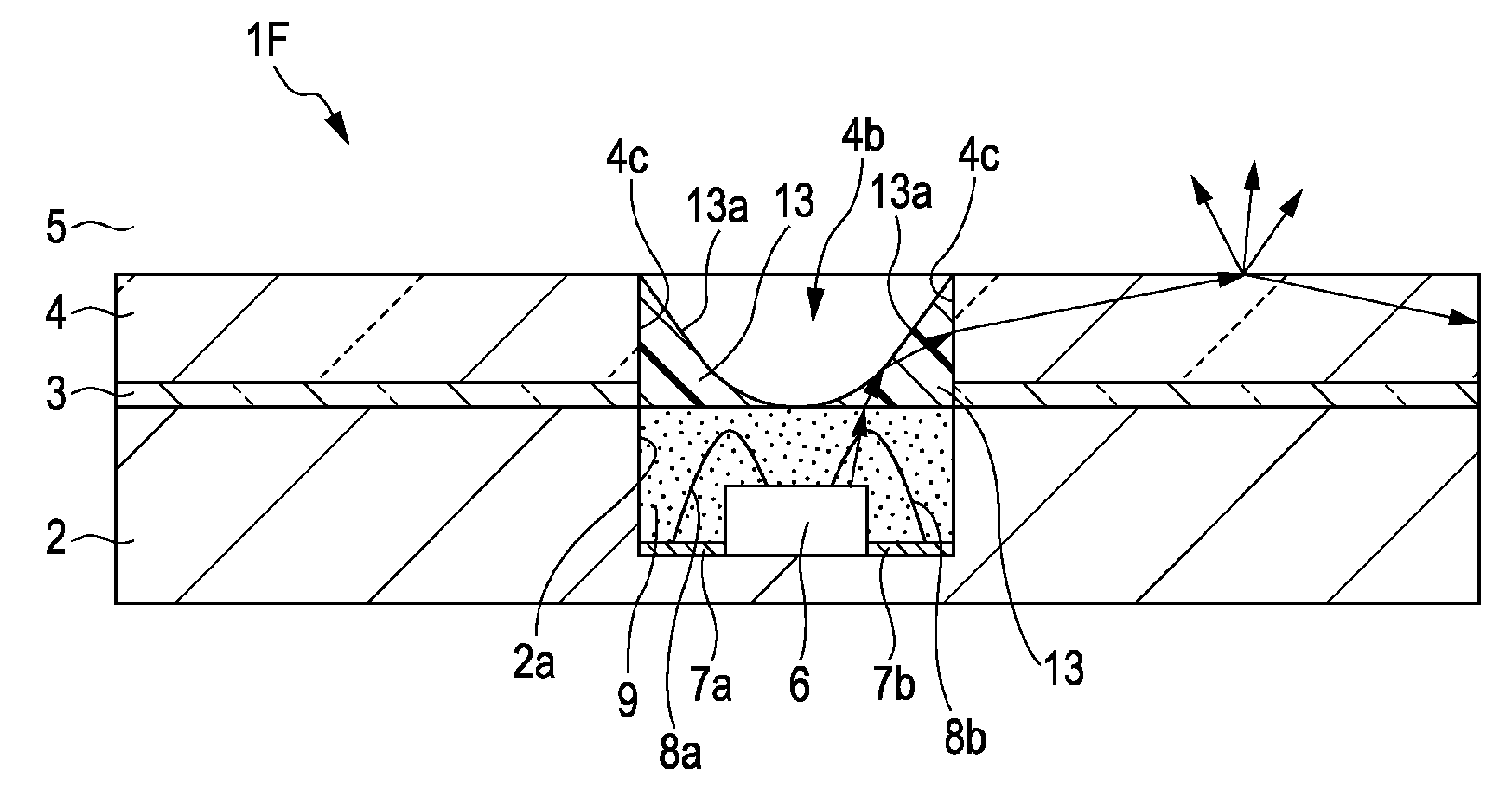
[0063]FIG. 1 is a sectional view of an illumination device according to the present invention. FIG. 1 graphically shows the light passing in the light guide layer with an arrow mark, which applies to the subsequent embodiments.

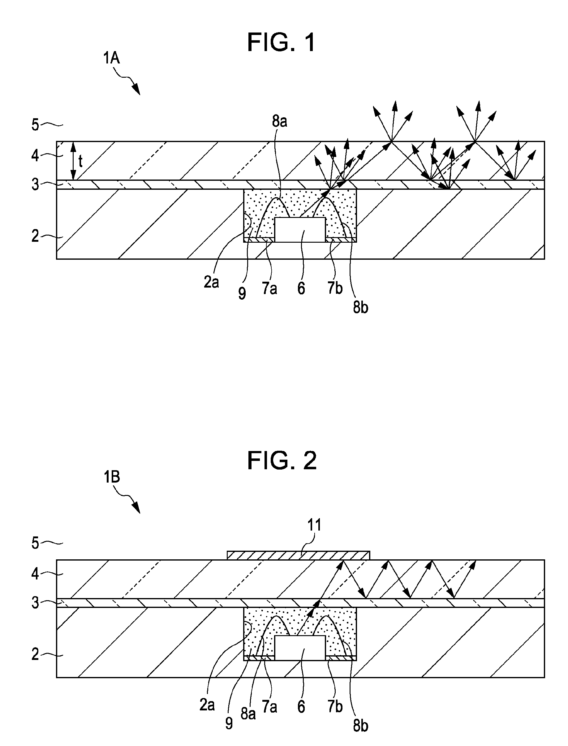
[0064]Referring to FIG. 1, an illumination device 1A includes a substrate 2 which may be the synthetic resin substrate that does not substantially deflect, the film-like synthetic resin substrate that can easily deflect, or the metal substrate.

[0065]The substrate 2 has a recess portion 2a formed in the surface, and a bare chip (light source) 6 as an optical element accommodated to be fixed in the recess portion 2a with the adhesive agent. Electrode layers of the bare chip 6 are individually coupled (wire bonding) with conductive patterns 7a and 7b formed on the bottom of the recess portion 2a via thin conductive wires 8a and 8b, respectively. A sealant 9 formed of the clear synthetic resin is filled in the recess portion 2a so as to seal the bare chip 6 and th...

second embodiment

[0075]The illumination device 1B of the second embodiment prevents the leakage of the light at the center opposite the bare chip 6, which allows more light to be guided to the circumferential location. Accordingly, the difference in the light intensity between the center and the circumferential location may be reduced. That is, the illumination device 1B may be of surface-emitting type for uniform emission.

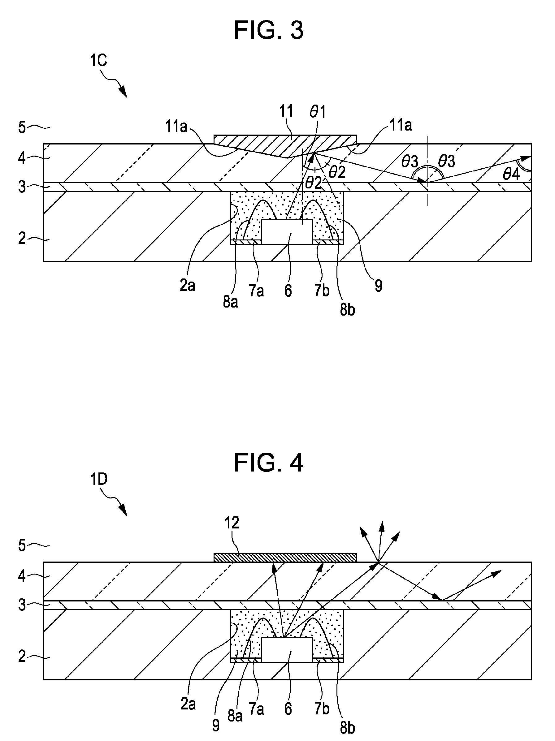
[0076]An illumination device 1C shown in FIG. 3 as the modified example of the second embodiment shown in FIG. 2 has the similar structure to the illumination device 1B except that the lower surface (reflection surface) of the mirror member 11 has tapered surfaces 11a, 11a. That is, the reflection surfaces 11a form an inverted cone shape, or an inverted pyramid shape having the center with the largest thickness and the peripheral sections each having the thickness gradually decreased as it is remote from the center.

[0077]In the modified example shown in FIG. 3, of the light irradi...

third embodiment

[0078]FIG. 4 is a sectional view of an illumination device according to the present invention.

[0079]An illumination device 1D shown in FIG. 4 has substantially the same structure as that of the illumination device according to the second embodiment except that a light absorbing member 12 is disposed on the surface of the light guide layer 4 above the position opposite the recess portion 2a or the bare chip 6 instead of the mirror member 11.

[0080]The light absorbing member 12 may be formed as a black layer with uniformity. In this case, however, a large amount of light is absorbed, which may require more outputs of the light source (bare chip 6) for providing sufficient light to serve as the illumination device, thus deteriorating the efficiency. It is preferable to form the black dot pattern or black matrix pattern on the light absorbing member 12 so as to allow a part of the light to transmit therethrough. Such member may be obtained by forming a metal chrome film on the glass subs...


PUM


Abstract

A recess portion is formed in a substrate to accommodate a light emitting element so as to be sealed with a sealant. A light guide layer formed of a thin transparent resin film is fixed onto the substrate via an adhesive layer to realize an illuminating device with a thin structure. The light emitted from the light emitting element is irradiated into the light guide layer via the sealant and the adhesive layer. The light fully reflecting on the boundary surfaces between the light guide layer and the adhesive layer, and between the light guide layer and the air layer passes inside the light guide layer. Then the light which has not fully reflected leaks outside from the surface of the transparent resin film which forms the light guide layer. This makes it possible to illuminate the surface of the illumination device 1A entirely with brightness.

Description

CLAIM OF PRIORITY[0001]This application claims benefit of the Japanese Patent Application No. 2007-005676 filed on Jan. 15, 2007, which is hereby incorporated by reference.BACKGROUND OF THE INVENTION[0002]1. Field of the Invention[0003]The present invention relates to an illumination device for illuminating an operation unit for various types of electronic devices, and more particularly, to a thin illumination device capable of effectively utilizing the light emitted from a light source, and an input device equipped with the illumination device.[0004]2. Description of the Related Art[0005]An electronic device of such type as audio equipment and a mobile electronic device is provided with a light guide member for guiding the light emitted from the light source such as the LED to the operation surface so as to illuminate the operation button, the fixed letter marked on the operation surface and the display unit having numbers displayed thereon.[0006]Generally, the illumination device ...

Claims


Application Information

Patent Timeline
Patent Type & Authority Applications(United States)
IPC IPC(8): F21V8/00F21S6/00F21V7/00F21V5/00
CPCG02B6/0018G02B6/002G02B6/0028H01L33/58H01H13/83H01H2219/062G02B6/0031H01L2224/48091H01L2924/181
Inventor ITO, NAOKIOKAMOTO, JUN
Owner ALPS ALPINE CO LTD
Why Eureka
Try Eureka