Method and apparatus for manufacturing device

a manufacturing device and manufacturing method technology, applied in electrical devices, semiconductor devices, capacitors, etc., can solve the problems of complex apparatus structure and complicated processes, and achieve the effects of reducing manufacturing process cost, reducing manufacturing time, and eliminating the number of manufacturing processes

Inactive Publication Date: 2009-11-05
ULVAC INC +1
View PDF3 Cites 174 Cited by
  • Summary
  • Abstract
  • Description
  • Claims
  • Application Information

AI Technical Summary

Benefits of technology

[0022]According to the method for manufacturing a device of the invention, the method includes: the process D in which the mask having a predetermined pattern is formed on the second electrode layer; the process E in which the first electrode layer, the ferroelectric layer, and the second electrode layer are selectively removed using the mask, the memory element is thereby formed; and the process F in which the mask is removed. In the processes D, E, and F, since at least, the processes D and E, or the processes E and F are continuously performed under reduced pressure, the number of the manufacturing processes is eliminated, a manufacturing time can be shortened, and it is possible to reduce the cost of the manufacturing process. Therefore, it is possible to effectively manufacture a device at a low cost in a short time as compared with conventional met

Problems solved by technology

There are problems in that such processes are co

Method used


Image

  • Method and apparatus for manufacturing device
  • Method and apparatus for manufacturing device
  • Method and apparatus for manufacturing device

Examples


Embodiment Construction

[0026]A method and an apparatus for manufacturing a device of the invention of an embodiment will be described.

[0027]In this embodiment, in order to easily understand the spirit of invention, the invention is specifically described. However, the invention is not limited to this embodiment without designation in particular. In addition, in these drawings which are utilized in the following explanation, appropriate changes have been made in the scale of the various members, in order to represent them at scales at which they can be easily understood.

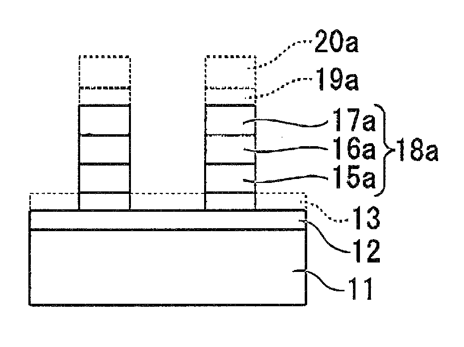
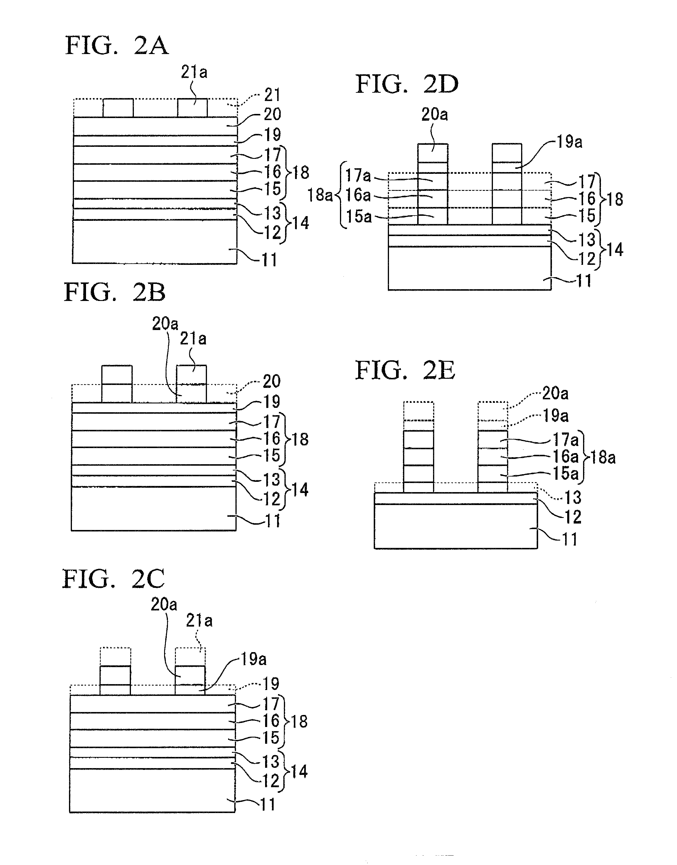
[0028]FIG. 1 is a schematic view showing an apparatus in which etching is performed at a normal temperature and at a high temperature, that is, an apparatus for manufacturing a device of an embodiment of the invention (hereinafter, referred as normal-temperature and high-temperature etching apparatus).

[0029]This normal-temperature and high-temperature etching apparatus 1 is an apparatus forming a device that has a layered structure in which...


PUM

PropertyMeasurementUnit
Temperatureaaaaaaaaaa
Pressureaaaaaaaaaa

Abstract

A method for manufacturing a device, includes: (A) forming a first electrode layer on a substrate; (B) forming a ferroelectric layer on the first electrode layer; (C) forming a second electrode layer on the ferroelectric layer; (D) forming a mask having a predetermined pattern on the second electrode layer; (E) forming a memory element by selectively removing the first electrode layer, the ferroelectric layer, and the second electrode layer using the mask; and (F) removing the mask, where at least, the processes (D) and (E), or the processes (E) and (F) are continuously performed under a reduced pressure.

Description

[0001]The entire disclosure of Japanese Patent Application No. 2008-112704, filed Apr. 23, 2008, is expressly incorporated by reference herein.BACKGROUND OF THE INVENTION[0002]1. Field of the Invention[0003]The present invention relates to a method and an apparatus for manufacturing a device. More specifically, the invention relates to a preferred method and a preferred apparatus for manufacturing devices used when a memory element of a ferroelectric memory referred to as a FeRAM (Ferroelectric Random Access Memory), or devices such as, a sensor, an actuator, an oscillator, a filter, a piezo element are formed.[0004]This application is based on and claims priority from Japanese Patent Application No. 2008-112704, filed on Apr. 23, 2008, the contents of which are incorporated herein by reference.[0005]2. Background Art[0006]Conventionally, as a type of nonvolatile memory, ferroelectric memory which is referred to as a FeRAM (ferroelectric random access memory) is known. In the ferroe...

Claims


Application Information

Patent Timeline
IPC IPC(8): H01L21/28H01L43/12H01L21/306
CPCH01L21/31116H01L28/55H01L21/32135H01L21/31122
Inventor TAKANO, KATSUOKOKUBUN, TAKESHIKOKAZE, YUTAKAUEDA, MASAHISAENDOU, MITSUHIROSUU, KOUKOUMIYAZAKI, TOSHIYANAKAMURA, TOSHIYUKI
Owner ULVAC INC
Why Eureka
Try Eureka