Test and burn-in socket for integrated circuits (ICS)
a technology of integrated circuits and sockets, which is applied in the field of sockets for an lga (land), can solve the problems of deterioration of quality, increased cost, and difficult assembly, and achieve the effect of easy treatment of components and increased component productivity and uniformity
- Summary
- Abstract
- Description
- Claims
- Application Information
AI Technical Summary
Benefits of technology
Problems solved by technology
Method used
Image
Examples
first embodiment
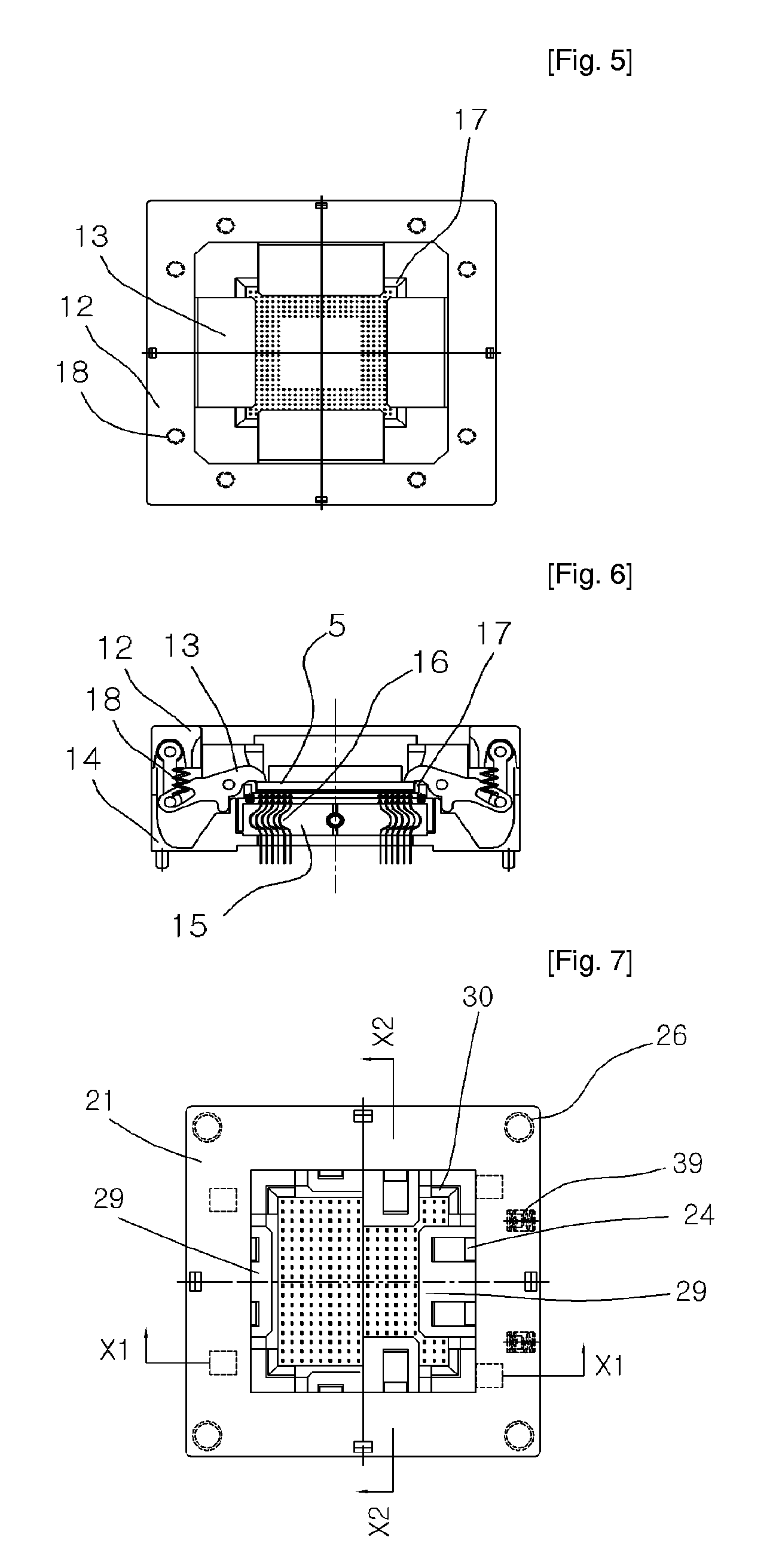
[0061]As shown in FIGS. 7 to 9, a body 37 of the test and burn-in socket for ICs, according to the present invention, includes a plurality of contact support holes 42 and a plurality of positioning pins 49. The contact support holes 42 receive and support a plurality of contacts 33 therein. The positioning pins 49 secure the socket body to a predetermined position on a PCB. In this case, the socket body 37 serves as a base for assembling a slide 35, a latch 29, a contact guide 31, and a cover 21.
[0062]A lead guide 36 is provided under the socket body 37. Lead guide holes 40 are positioned at ends of lower contact terminals 63 of the contacts, via the lead guide 36.
[0063]The lead guide 36 functions to maintain the lower contact terminals 63 in a straight line without bending the lower contact terminals 63. Further, when the socket is assembled with the PCB, the lead guide 36 functions to precisely insert the lower contact terminals 63 into through holes of the PCB. When the socket is...
second embodiment
[0109]According to the present invention, the test and burn-in socket for ICs is a surface-mount-type socket.
[0110]Hereinbefore, the test and burn-in socket for ICs, according to the first embodiment of this invention, has been described. Hereinafter, a test and burn-in socket for ICs, according to the second embodiment of this invention, will be described with reference to FIGS. 29 and 30. FIG. 29 is a plan view of a test and burn-in socket for ICs, according to the third embodiment of the present invention, and FIG. 30 is a vertical sectional view taken along line X5-X5 of FIG. 29.
third embodiment
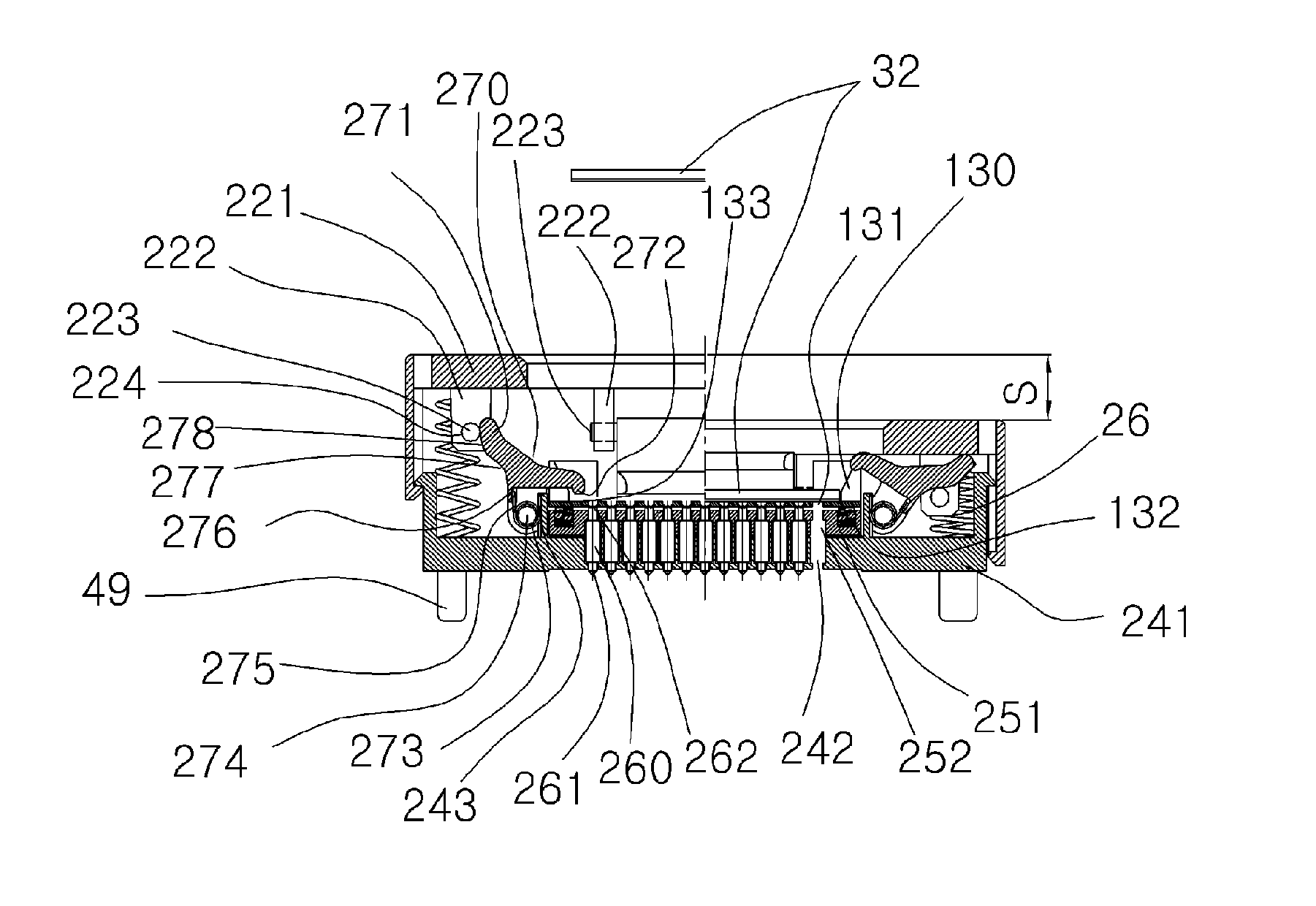
[0111]As shown in FIGS. 29 and 30, the socket according to the present invention is a socket using pogo contacts. Each pogo contact includes a contact body 160 accommodating a spring having a predetermined elastic force therein, a lower terminal 161, and an upper terminal 162. The lower terminal 161 and the upper terminal 162 are operated by the spring.
[0112]As shown in FIGS. 29 and 30, a socket body 141 is provided with a plurality of bolt insert holes 99 to be fastened to terminals formed on a PCB using bolts. A plurality of holes 142 and a plurality of positioning pins 49 are formed in the lower portion of the socket body 141. Lower terminals 161 of the pogo contacts pass through the holes 142. Further, the holes 142 are formed to prevent the contact bodies 160 from being dislodged from predetermined positions. The positioning pins 49 secure the socket body to a predetermined position on the PCB. Preferably, the socket body 141 serves as a base for assembling a latch 29, a contac...
PUM
 Abstract
Description
Claims
Application Information


