Assessment method for process improvement decisions

Inactive Publication Date: 2009-11-05
INOTERA MEMORIES INC
View PDF0 Cites 27 Cited by
  • Summary
  • Abstract
  • Description
  • Claims
  • Application Information

AI Technical Summary

Benefits of technology

[0008]Therefore, the objective of the present invention is to provide an assessment method for process improvement decisions, which offers assessment evaluation and process improvement decision rega

Problems solved by technology

However, when using the prior art Failure Mode and Effects Analysis in the semiconductor processes, since the Occurrence 104 (O) and the Detection 106 (D) may not be acquired in advance before the change of semiconductor process, which accordingly

Method used


Image

  • Assessment method for process improvement decisions
  • Assessment method for process improvement decisions
  • Assessment method for process improvement decisions

Examples


Embodiment Construction

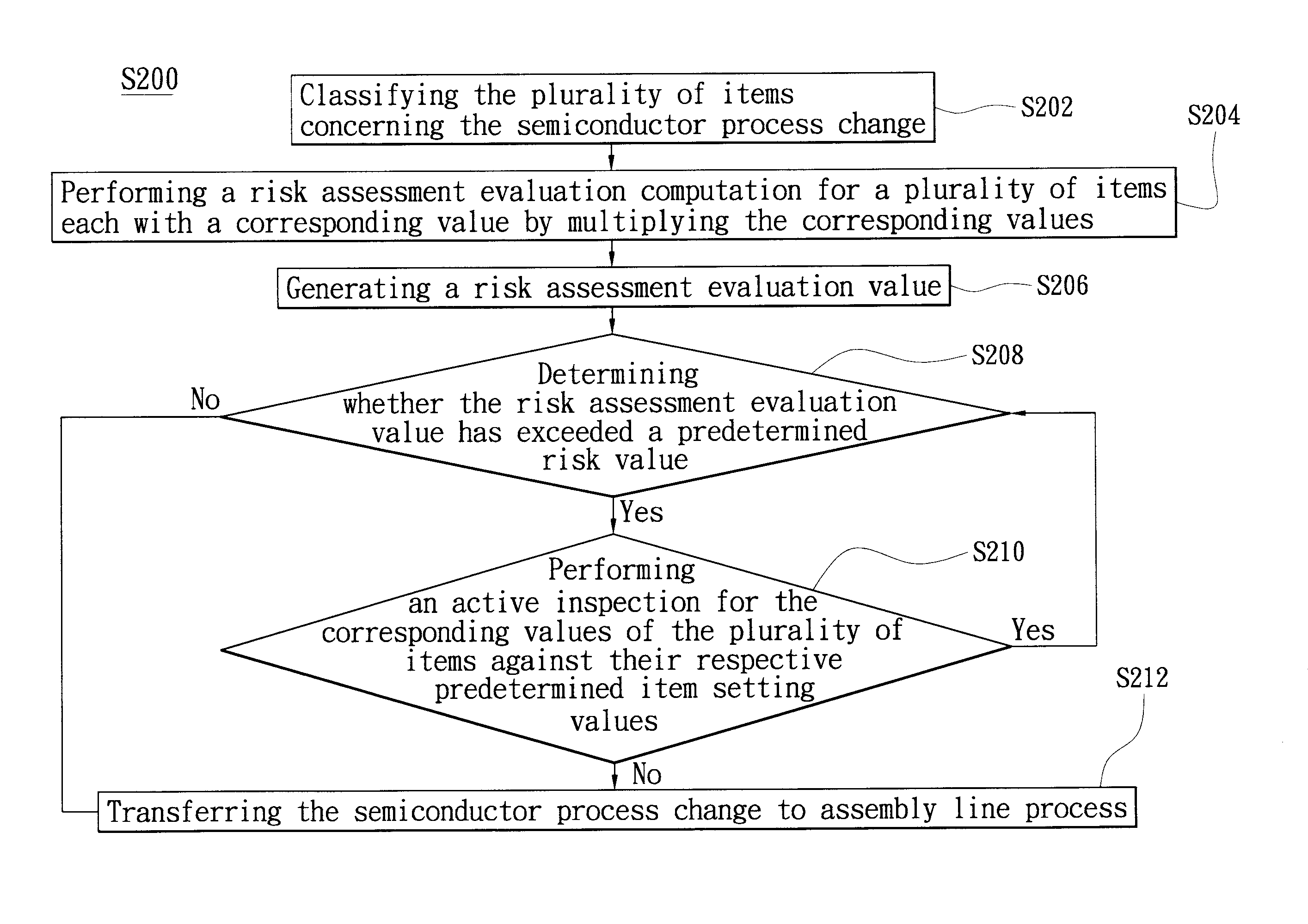
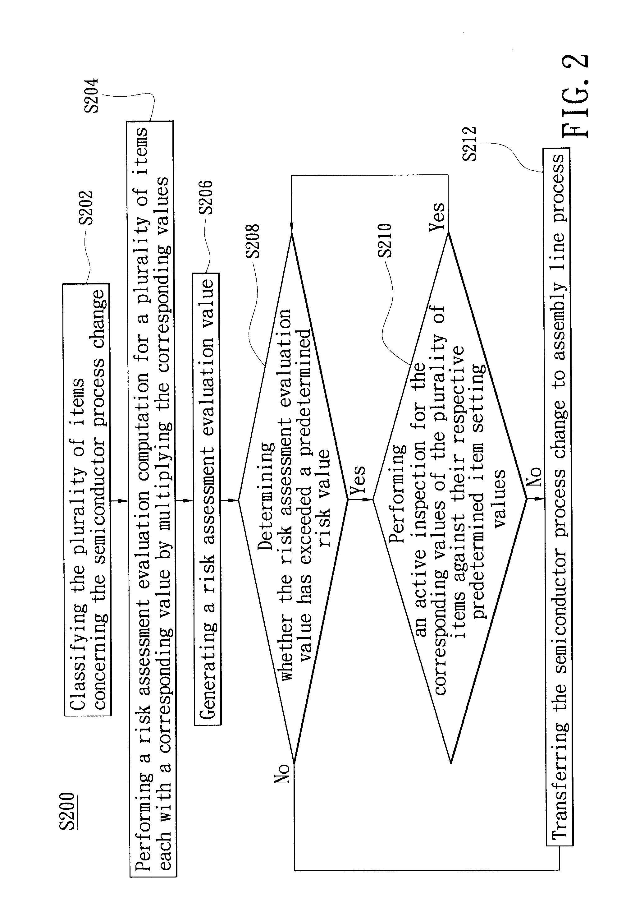
[0026]Refer now to FIG. 2, wherein the present invention provides an assessment method S200 for process improvement decisions which is applicable to a semiconductor process change, comprising the following steps: step S202, step S204, step S206, step S208, step S210 and step S212.

[0027]The execution of the step S202 consists of classifying the plurality of items concerning the semiconductor process change, in which, with reference to FIGS. 3A to 3D, these items include an EXPERIENCE 310, an INFLUENCE AREA 320 and an AGGRESSIVE CHECK POINT 330. The value to which the EXPERIENCE 310 corresponds is a confidence value 312, in which the EXPERIENCE 310 includes QD ECN (Quality Design with Engineering Change Note: there exist other factories of the same category), QD PILOT / IMI SWR (Quality Design PILOT / Incoming Material Inspection of Semiconductor Wafer Representation: batch experiment in median / small quantity during experiment), SUPPORTING ANALYSIS or NO EXPERIENCE, and the confidence val...


PUM


Abstract

A risk assessment method for process improvement decisions applying for semiconductor process change comprises: performing a risk assessment evaluation to compute a polarity (plurality?) of items corresponding to their values, generating a risk assessment evaluation value to determine if the risk assessment evaluation value is in a risk setting value, go to next two steps; not, go to next step; performing an active inspect for the polarity (plurality?) of items corresponding to their item setting values, if not satisfied with the active inspect, repeat the above step; if not, transferring the semiconductor process change to online process.

Description

BACKGROUND OF THE INVENTION[0001]1. Field of the Invention[0002]The present invention generally relates to an assessment method for process improvement decisions; in particular, it relates to an assessment method for process improvement decisions in the field of semiconductor process change application.[0003]2. Description of Related Art[0004]In current semiconductor foundries for integrated circuit manufacture, it has become one of the most essential key points for present semiconductor foundries to find applicable approaches for full exploitation on the performance of production facility management, advancement in high reliability for process equipment improvement, reduction of influence brought on by process failure risks, in order to control and lessen the damage induced by occurrence of such failures, which are also the most effective paths to increase product yield rate as well as to enhance the competitiveness of semiconductor foundries in semiconductor fabrication.[0005]The ...

Claims


Application Information

Patent Timeline
IPC IPC(8): G06Q10/00
CPCG06Q10/0635G06Q10/06
Inventor CHEN, SHIH-LUNG
Owner INOTERA MEMORIES INC
Why Eureka
Try Eureka