Method and structure, using flexible membrane surfaces, for setting and/or maintaining a uniform micron/sub-micron gap separation between juxtaposed photosensitive and heat-supplying surfaces of photovoltaic chips and the like for the generation of electrical power

a photovoltaic chip and photosensitive surface technology, applied in the field of nearfield devices, can solve the problems of bow and surface irregularities of each chip, the difficulty of achieving gap uniformity, and the difficulty of accommodating the irregularities of the chip

Active Publication Date: 2009-11-12
MTPV POWER CORP
View PDF4 Cites 27 Cited by
  • Summary
  • Abstract
  • Description
  • Claims
  • Application Information

AI Technical Summary

Problems solved by technology

There are, however, several challenges faced in attaining gap uniformity, caused by bowing or irregular surfaces, or applied external forces when manufacturing such near-field systems, particularly those that are to be capable of generating commercially significant (>1 kW) power levels.
In such embodiment, indeed, resulting bow and surface irregularities of each chip must be accommodated during assembly.

Method used


Image

  • Method and structure, using flexible membrane surfaces, for setting and/or maintaining a uniform micron/sub-micron gap separation between juxtaposed photosensitive and heat-supplying surfaces of photovoltaic chips and the like for the generation of electrical power
  • Method and structure, using flexible membrane surfaces, for setting and/or maintaining a uniform micron/sub-micron gap separation between juxtaposed photosensitive and heat-supplying surfaces of photovoltaic chips and the like for the generation of electrical power
  • Method and structure, using flexible membrane surfaces, for setting and/or maintaining a uniform micron/sub-micron gap separation between juxtaposed photosensitive and heat-supplying surfaces of photovoltaic chips and the like for the generation of electrical power

Examples


Embodiment Construction

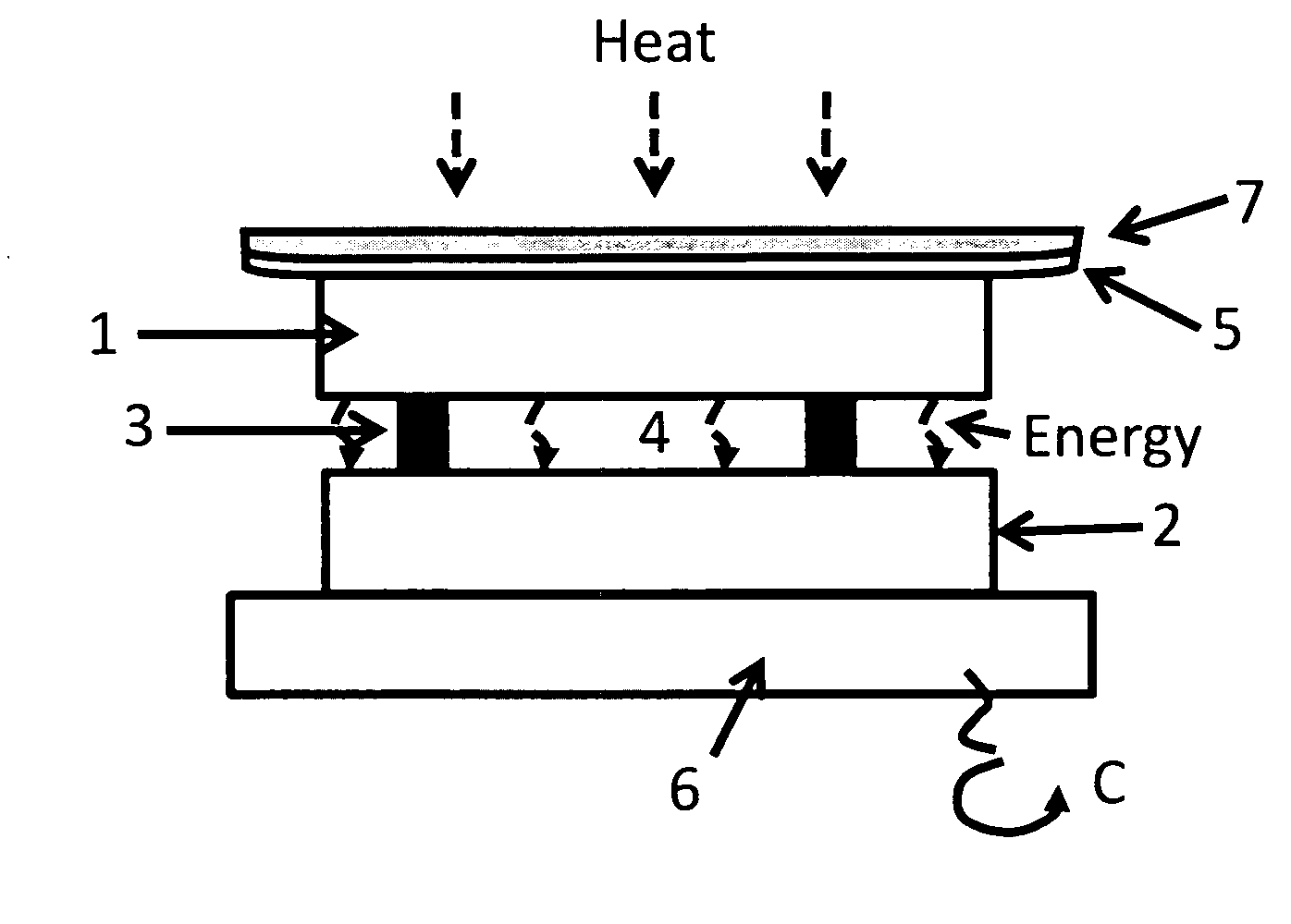
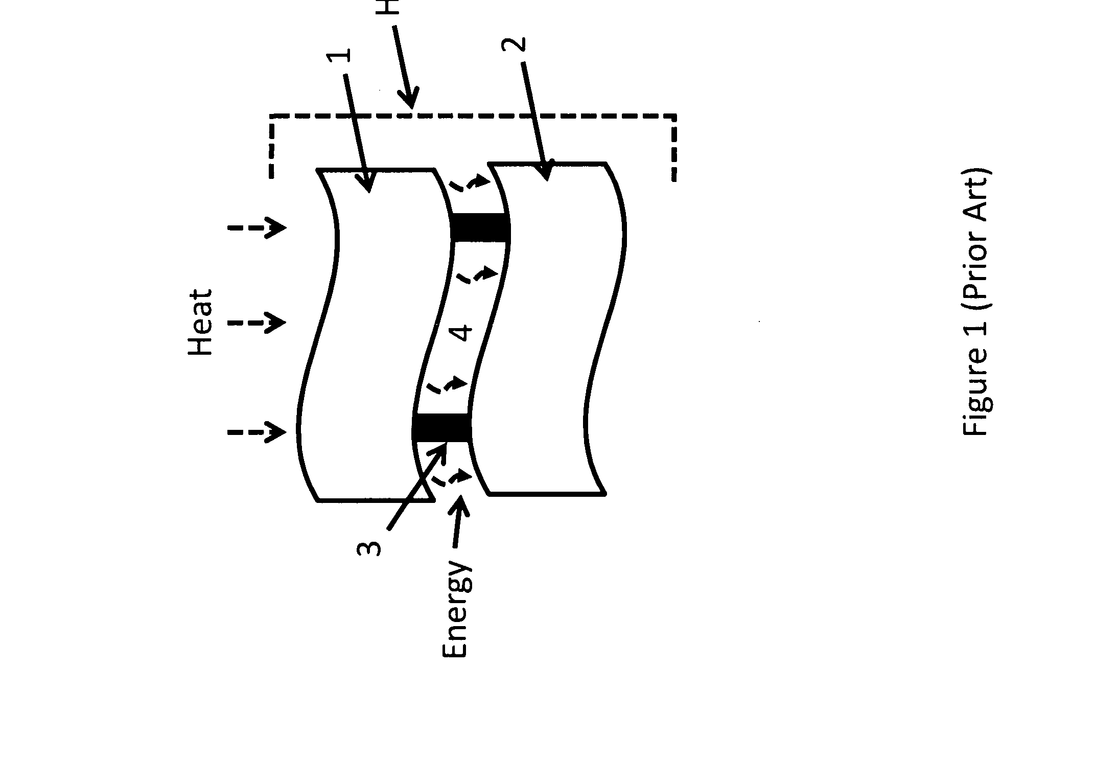
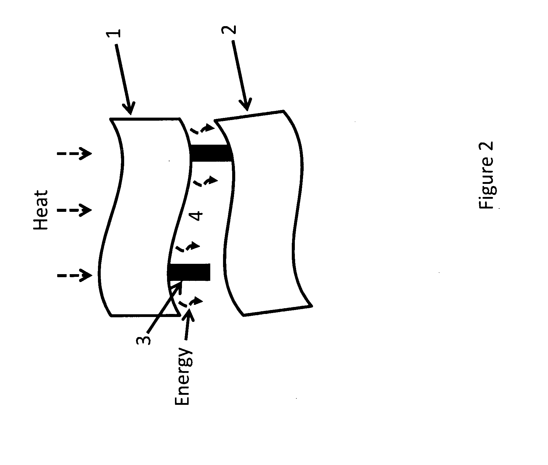
[0023]A general fragmentary schematic of a near-field system is presented in in FIG. 1, comprised of a thermal emitter 1, a radiation receiver 2, one or more spacers 3, and a sub-micron gap 4, preferably in an evacuated housing H. The spacers define the size of the gap between the emitter and receiver and may be fabricated on either or both the emitter or receiver. The size of the gap is preferably less than one micron—for example, less than 100 nanometers. Incoming heat increases the temperature of the emitter 1 and causes it to emit energy. In MTPV, this energy takes the form of infrared radiation according to Planck's Law and is generally in the infrared (1-2 micrometer wavelength) regime. In CC, this energy takes the form of electrical fields active over very small distances (4 and is absorbed by the receiver 2. In MTPV, the receiver 2 is a photovoltaic cell. In CC, the receiver 2 may be one or more two-level quantum dots separated from a reservoir by a tunneling barrier and con...


PUM


Abstract

A near-field energy conversion structure and method of assembling the same, utilizing a sub-micrometer “near field” gap between juxtaposed photocell infrared radiation receiver and heat emitter surfaces, wherein compliant membrane structures, preferably fluid-filled, are interposed in the structure.

Description

FIELD OF INVENTION[0001]The present invention is concerned with the field of near-field devices for the generation of electric current and power through transfer of energy from an emitter across a non-isothermal gap to a receiver, being more specifically directed to such devices using micron and submicron gap (“near-field”) separations and the maintaining of the uniformity of the separation of such gaps between juxtaposed receiver and emitter structures for such use; and thereby achieving photocurrents many times those obtained in conventional (“far field”) devices, as described in U.S. Pat. Nos. 6,084,173 and 6,232,546, Patent Publication No. 2004 / 003172A1 of Nov. 25, 2004 and in a paper entitled “Micron-gap Thermo Photo Voltaic (MTPV)”, DiMatteo et al, Proceedings of the Fifth TPV Conference, 2002, all incorporated herein by reference.BACKGROUND OF INVENTION[0002]There exists a class of novel electronic devices that utilize energy transfer between a relatively hot and a relatively...

Claims


Application Information

Patent Timeline
Patent Type & Authority Applications(United States)
IPC IPC(8): H01L37/00H01L35/34
CPCH02S10/30H01L31/024Y02E10/50
Inventor GREIFF, PAULDIMATTEO, ROBERTBROWN, ERICLEITZ, CHRISTOPHER
Owner MTPV POWER CORP
Why Eureka
Try Eureka