Semiconductor light-emitting device

a technology of semiconductors and light-emitting devices, which is applied in the direction of semiconductor/solid-state device manufacturing, semiconductor devices, electrical devices, etc., can solve the problems that documents 3 to 5 still have not achieved sufficient light extraction efficiency, and achieve the effect of improving light extraction efficiency

Active Publication Date: 2009-11-12
PANASONIC CORP
View PDF5 Cites 70 Cited by
  • Summary
  • Abstract
  • Description
  • Claims
  • Application Information

AI Technical Summary

Benefits of technology

[0011]The present invention provides a semiconductor light-emitting device whose light extraction efficiency is improved.

Problems solved by technology

However, when using the epoxy resin or the silicone resin as the binder for the phosphor layer in the conventional semiconductor light-emitting device described above, there arise the following problems.
However, the methods proposed in Patent documents 3 to 5 still have not achieved the light extraction efficiency sufficient for the application to an illuminating apparatus or the like, for example.

Method used


Image

  • Semiconductor light-emitting device
  • Semiconductor light-emitting device
  • Semiconductor light-emitting device

Examples


embodiment 1

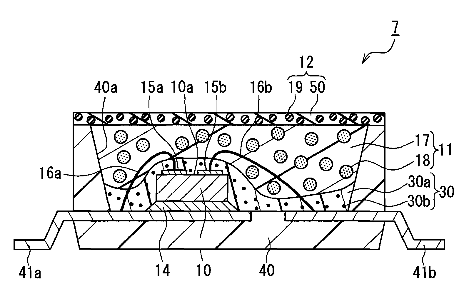
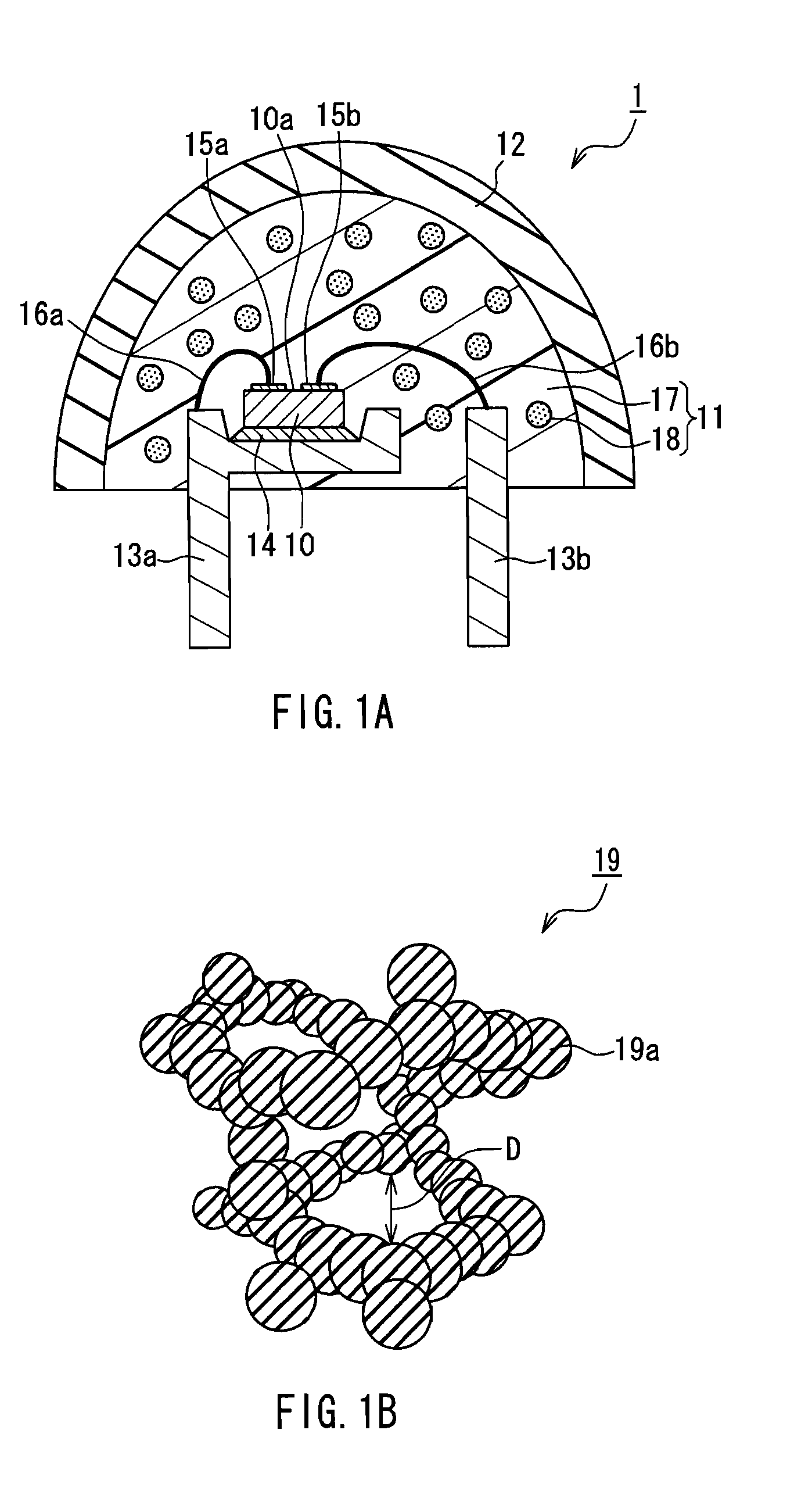
[0046]First, a semiconductor light-emitting device according to Embodiment 1 of the present invention will be described. FIG. 1A is a sectional view showing the semiconductor light-emitting device according to Embodiment 1 of the present invention, and FIG. 1B is a schematic view showing a constituent material of an outer layer included in the semiconductor light-emitting device shown in FIG. 1A.

[0047]As shown in FIG. 1A, a semiconductor light-emitting device 1 includes a semiconductor light-emitting element 10, a phosphor layer 11 that is formed so as to cover the semiconductor light-emitting element 10, and an outer layer 12 that is formed so as to cover the phosphor layer 11. The semiconductor light-emitting element 10 is fixed firmly on a bottom surface of a cup-like recessed portion provided at an end of a first lead frame 13a using a fixing paste material 14 formed of an Ag paste or the like.

[0048]A light extraction surface 10a of the semiconductor light-emitting element 10 is...

embodiment 2

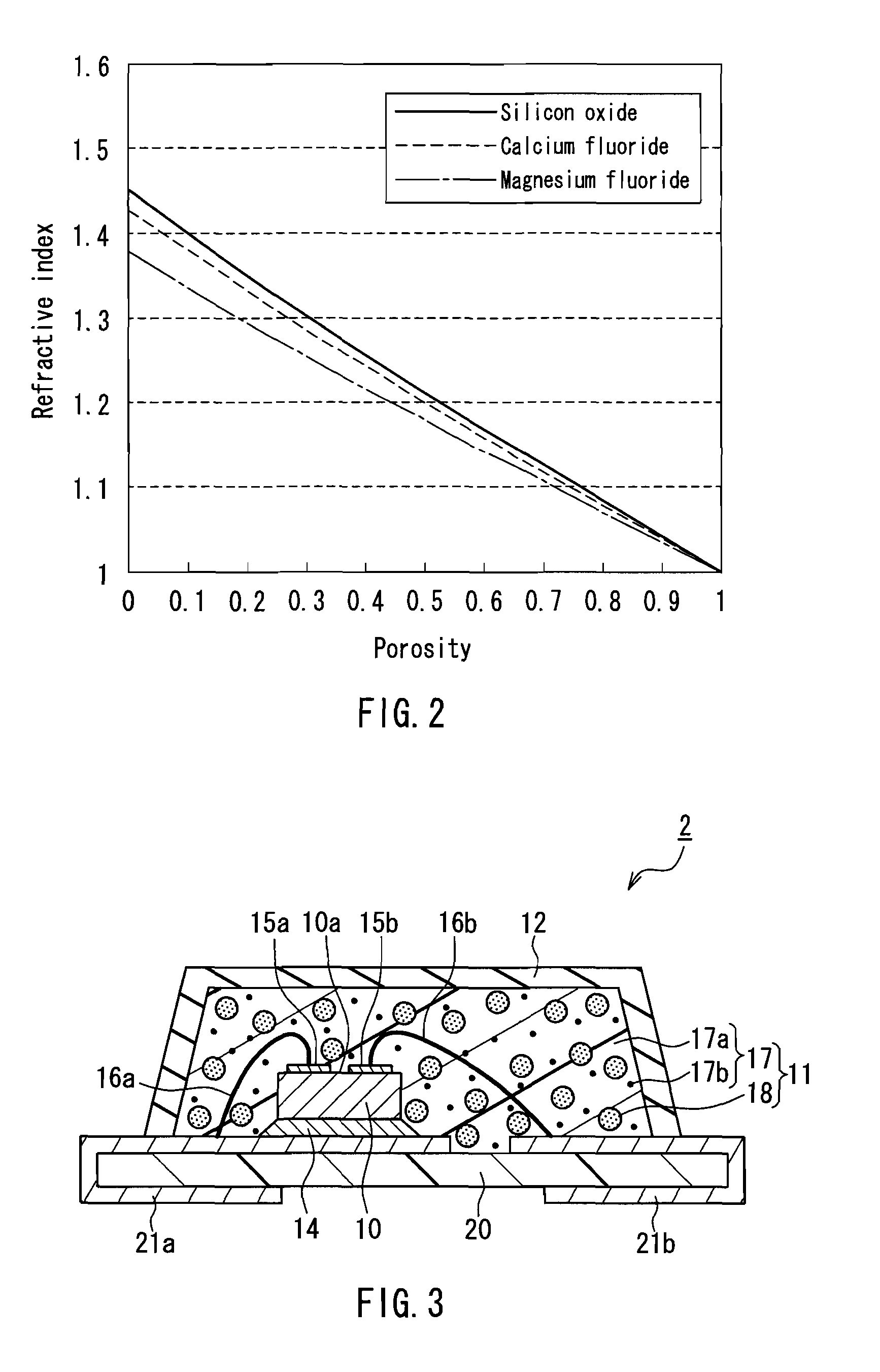
[0064]Now, a semiconductor light-emitting device according to Embodiment 2 of the present invention will be described. FIG. 3 is a sectional view showing the semiconductor light-emitting device according to Embodiment 2 of the present invention.

[0065]As shown in FIG. 3, in a semiconductor light-emitting device 2, a semiconductor light-emitting element 10 is mounted on a substrate 20. The substrate 20 is provided with a first wiring 21a and a second wiring 21b. The first wiring 21a and the second wiring 21b are connected electrically with a first electrode 15a and a second electrode 15b via a first wire 16a and a second wire 16b, respectively.

[0066]Further, a binder 17 in a phosphor layer 11 is formed of a composite material containing a binder material 17a and an inorganic particle 17b having an effective particle diameter equal to or smaller than a quarter of a wavelength of light passing through the binder material 17a. The inorganic particle 17b has a higher refractive index than...

embodiment 3

[0074]Now, a semiconductor light-emitting device according to Embodiment 3 of the present invention will be described. FIG. 7 is a sectional view showing the semiconductor light-emitting device according to Embodiment 3 of the present invention.

[0075]As shown in FIG. 7, a semiconductor light-emitting device 3 further includes a light-transmitting layer 30 that is interposed between the semiconductor light-emitting element 10 and the phosphor layer 11, in addition to the configuration of the semiconductor light-emitting device 1 according to Embodiment 1 described above. This makes it possible not only to produce an effect similar to the semiconductor light-emitting device 1 but also to prevent the deterioration of the phosphor layer 11 due to heat generated from the semiconductor light-emitting element 10, because the semiconductor light-emitting element 10 and the phosphor layer 11 are not in contact with each other.

[0076]It is preferable that the refractive index of the light-tran...


PUM


Abstract

Disclosed is a semiconductor light-emitting device having improved light-extraction efficiency. Specifically disclosed is a semiconductor light-emitting device (1) comprising a semiconductor light-emitting element (10), a phosphor layer (11) which is so formed as to cover at least a part of the semiconductor light-emitting element (10), and an outer layer (12) which is so formed as to cover at least a part of the phosphor layer (11). The phosphor layer (11) contains a binder (17) and a phosphor (18) dispersed in the binder (17), and the outer layer (12) contains a porous material (19). Consequently, the semiconductor light-emitting device is improved in light-extraction efficiency.

Description

TECHNICAL FIELD[0001]The present invention relates to a semiconductor light-emitting device including a semiconductor light-emitting element.BACKGROUND ART[0002]As semiconductor light-emitting elements including a semiconductor multilayer film, light emitting diodes (in the following, referred to as “LEDs”) have been known. Among them, LEDs emitting blue light such as GaN LEDs can be combined with a phosphor that is excited by blue light and emits fluorescence, and thereby applied to semiconductor light-emitting devices emitting white light.[0003]FIG. 12 is a sectional view showing a conventional semiconductor light-emitting device emitting white light. As shown in FIG. 12, in a semiconductor light-emitting device 100, an LED chip 102 emitting blue light is fixed firmly on a bottom surface of a recessed portion provided at one end of a first lead frame 101a, using a chip fixing paste material 103 formed of an Ag paste or the like.[0004]An upper surface of the LED chip 102 is provide...

Claims


Application Information

Patent Timeline
Patent Type & Authority Applications(United States)
IPC IPC(8): H01L33/00H01L33/32H01L33/50H01L33/56
CPCH01L33/501H01L33/54H01L33/56H01L33/58H01L2224/13H01L2224/48091H01L2224/48257H01L2224/73265H01L2224/8592H01L2224/48247H01L2224/32257H01L2924/00014H01L2224/05568H01L2224/05573H01L2924/181H01L2224/05599H01L2924/00012
Inventor SUZUKI, MASA-AKI
Owner PANASONIC CORP
Why Eureka
Try Eureka