Pixel circuit and driving method thereof

a technology of pixel circuit and driving method, which is applied in the direction of non-linear optics, static indicating devices, instruments, etc., can solve the problems of reducing the efficiency of the driving circuit of the panel, and reducing the number of divided display regions

Inactive Publication Date: 2009-11-12
CHUNGHWA PICTURE TUBES LTD
View PDF4 Cites 68 Cited by
  • Summary
  • Abstract
  • Description
  • Claims
  • Application Information

AI Technical Summary

Benefits of technology

[0009]The present invention is directed to a pixel circuit. A transistor is added on a pixel electrode and an enabling signal of a gate line is used to conduct a bias of the pixel electrode to a gray level voltage or a common voltage so as to achieve the effect of black / gray frame insertion.

Problems solved by technology

As consumers demand more and more strictly of dynamic image quality, how to eliminate the blur effect caused by hold-type displays gradually becomes a primary issue.
However, the number of the divided display regions is limited by the resolution of the LCD panel and has its maximum.
However, since the panel requires a doubled number of gate lines and two sets of independent driving chips, the driving circuit of the panel is designed as more complicated and thereby costing more.

Method used


Image

  • Pixel circuit and driving method thereof
  • Pixel circuit and driving method thereof
  • Pixel circuit and driving method thereof

Examples


first embodiment

The First Embodiment

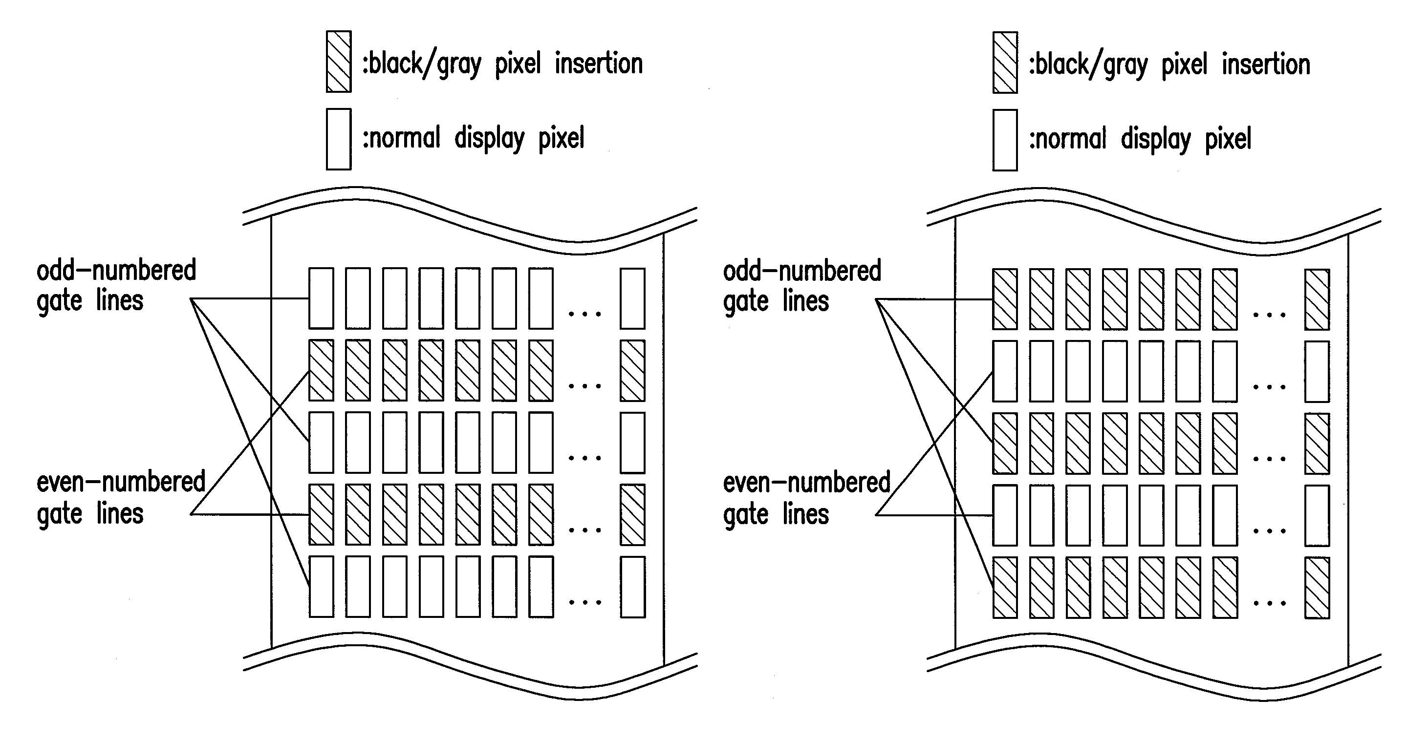
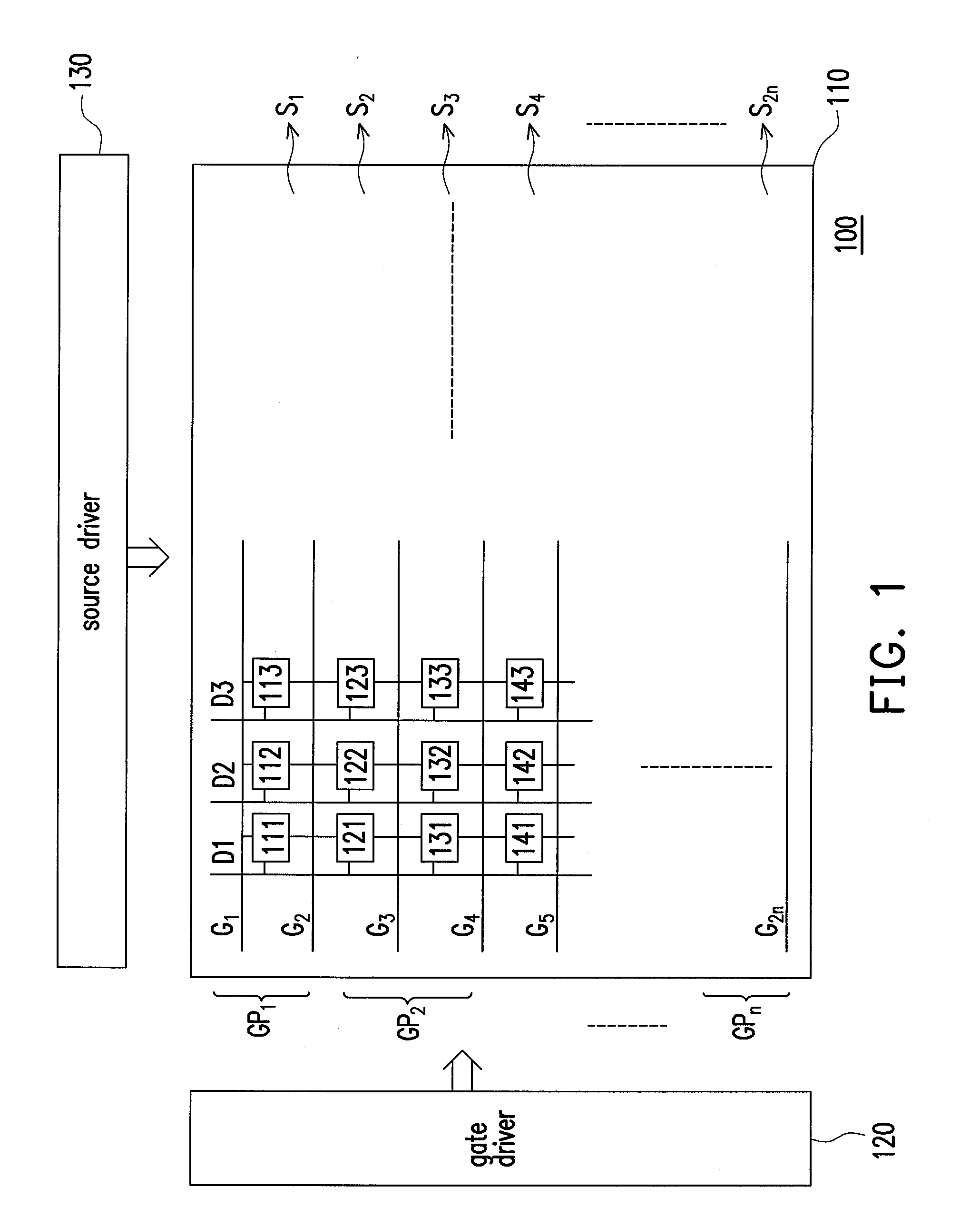
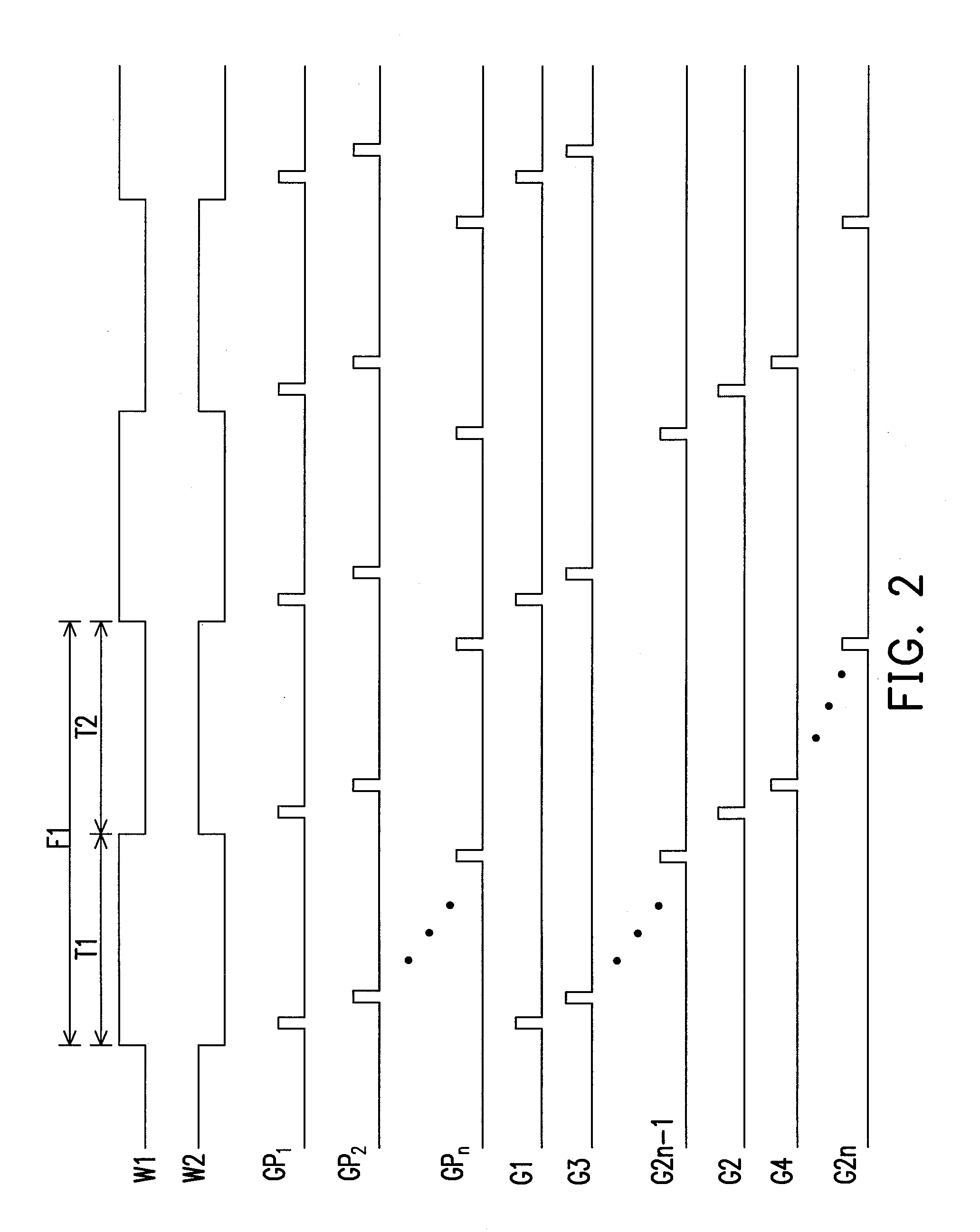
[0035]FIG. 1 is a circuit diagram of a display according to an embodiment of the present invention. A liquid crystal display (LCD) 100 includes a display panel 110, a gate driver 120 and a source driver 130. The display panel 110 includes pixel columns S1-S2n and gate lines G1-G2n; n is a positive integer. The gate driver 120 is used for transmitting gate scan signals, and the source driver 130 is used for transmitting pixel driving signals. In the present embodiment, all pixels corresponding to a gate line are represented by a pixel column. Accordingly, each of the pixel columns has a plurality of pixels and a pixel circuit represents an equivalent circuit of a pixel structure.

[0036]In the display panel 110, each of the pixel columns S1-S2n includes a plurality of pixel circuits (e.g. 111-113, 121-123, 131-133) and is electrically connected to adjacent gate lines G1-G2n over and under the pixel column correspondingly. Each of the gate lines G1-G2n is likewise el...

second embodiment

The Second Embodiment

[0042]Next, the pixel circuit of the present invention is further described using a pixel circuit 111 as an example. FIG. 5A illustrates a pixel circuit diagram according to the second embodiment of the present invention. A pixel circuit 500 shows one of a variety of embodiments for the pixel circuit 111. The pixel circuit 500 includes transistors TFT1 and TFT2, a pixel capacitor CLC and a storage capacitor CST and is electrically connected between adjacent gate lines G1 and G2. The pixel capacitor CLC and the storage capacitor CST have a common node 510. The other end of the pixel capacitor CLC is electrically connected to a common voltage VCOM (a ground voltage level or a specific voltage level), and the storage capacitor CST is electrically connected between the common node 510 and a gray level voltage VCS. The transistor TFT1 is electrically connected between the data line D1 and the common node 510, and a gate of the transistor TFT1 is electrically connecte...

third embodiment

The Third Embodiment

[0045]Thereafter, in the present invention, the circuit design concept disclosed by the second embodiment is applied to a variety of pixel structures. FIG. 6A is a pixel circuit diagram according to the third embodiment of the present invention. Likewise, the current location of the pixel circuit 111 is taken as an example, and a pixel circuit 600 illustrates another embodiment of the pixel circuit 111. The pixel circuit 600 includes transistors TFT1-TFT3, pixel capacitors CLC1 and CLC2 and storage capacitors CST1 and CST2. In the present embodiment, the pixel circuit 600 is mainly constituted by two sub-pixel structures. The pixel capacitor CLC1 and the storage capacitor CST1 form a sub-pixel. The pixel capacitor CLC2 and the storage capacitor CST2 form the other sub-pixel. Such pixel structure has various applications, for example, in LCDs with wide view angle.

[0046]A circuit structure consisting of the pixel capacitor CLC1, the storage capacitor CST1 and the t...


PUM


Abstract

A pixel circuit and a driving method thereof are provided. The pixel circuit includes a pixel capacitor, a storage capacitor, a first transistor and a second transistor. A common node is between the storage capacitor and the pixel capacitor. The first transistor is electrically connected between a data line and the common node, and a gate thereof is electrically connected to a first gate line. The second transistor is electrically connected between the common node and a gray level voltage, and a gate thereof is electrically connected to a second gate line. The first gate and the second gate line are adjacent.

Description

CROSS-REFERENCE TO RELATED APPLICATION[0001]This application claims the priority benefit of Taiwan application serial no. 97116989, filed May 8, 2008. The entirety of the above-mentioned patent application is hereby incorporated by reference herein and made a part of this specification.BACKGROUND OF THE INVENTION[0002]1. Field of the Invention[0003]The present invention relates to a black frame insertion technology, and particularly to a pixel circuit applied to black / gray frame insertion and a driving method thereof.[0004]2. Description of Related Art[0005]Demand for liquid crystal displays (LCDs) has been growing rapidly in recent years and development towards large sizes gradually becomes the trend. As the size of LCD panels increases, not only does the resolution thereof enhance but demand for television dynamic image display also significantly increases. Since the LCD is driven by a hold-type method rather than an impulse-type method of the cathode ray tube (CRT) and liquid cry...

Claims


Application Information

Patent Timeline
Patent Type & Authority Applications(United States)
IPC IPC(8): G09G3/36
CPCG02F1/133707G02F1/136213G02F1/13624G09G3/2025G09G3/2081G09G3/3659G09G2320/028G09G2300/0443G09G2300/0842G09G2300/0852G09G2310/0224G09G2310/0251G09G2320/0261G09G3/3677
Inventor WANG, HSIEN-CHUNHUANG, TZU-CHIEN
Owner CHUNGHWA PICTURE TUBES LTD
Why Eureka
Try Eureka