High performance optoelectronic device

a high-performance, optoelectronic technology, applied in the direction of semiconductor devices, basic electric elements, electrical apparatus, etc., can solve the problems of reducing the amount of photons incident to the n-type-doped layer, serious impact on the energy conversion efficiency of the cell, and not only complicating the fabricating process, so as to reduce production costs, reduce the amount of material, and simplify the process

Inactive Publication Date: 2009-11-19
TATUNG COMPANY +1
View PDF10 Cites 56 Cited by
  • Summary
  • Abstract
  • Description
  • Claims
  • Application Information

AI Technical Summary

Benefits of technology

[0024]The optoelectronic device of the present invention is fabricated by a

Problems solved by technology

As a consequence, the amount of the photons incident to the N-type-doped layer is reduced and the energy converting efficiency of the ce

Method used


Image

  • High performance optoelectronic device
  • High performance optoelectronic device
  • High performance optoelectronic device

Examples


Embodiment Construction

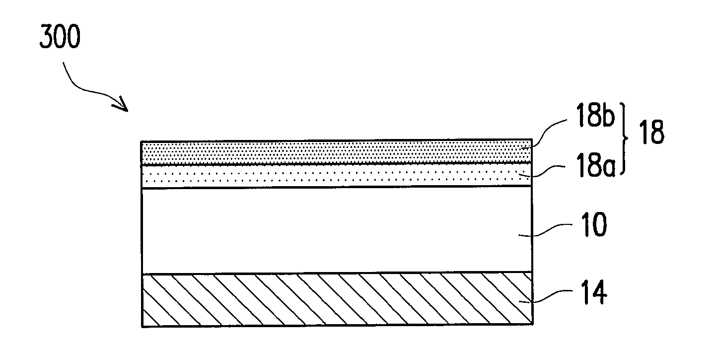
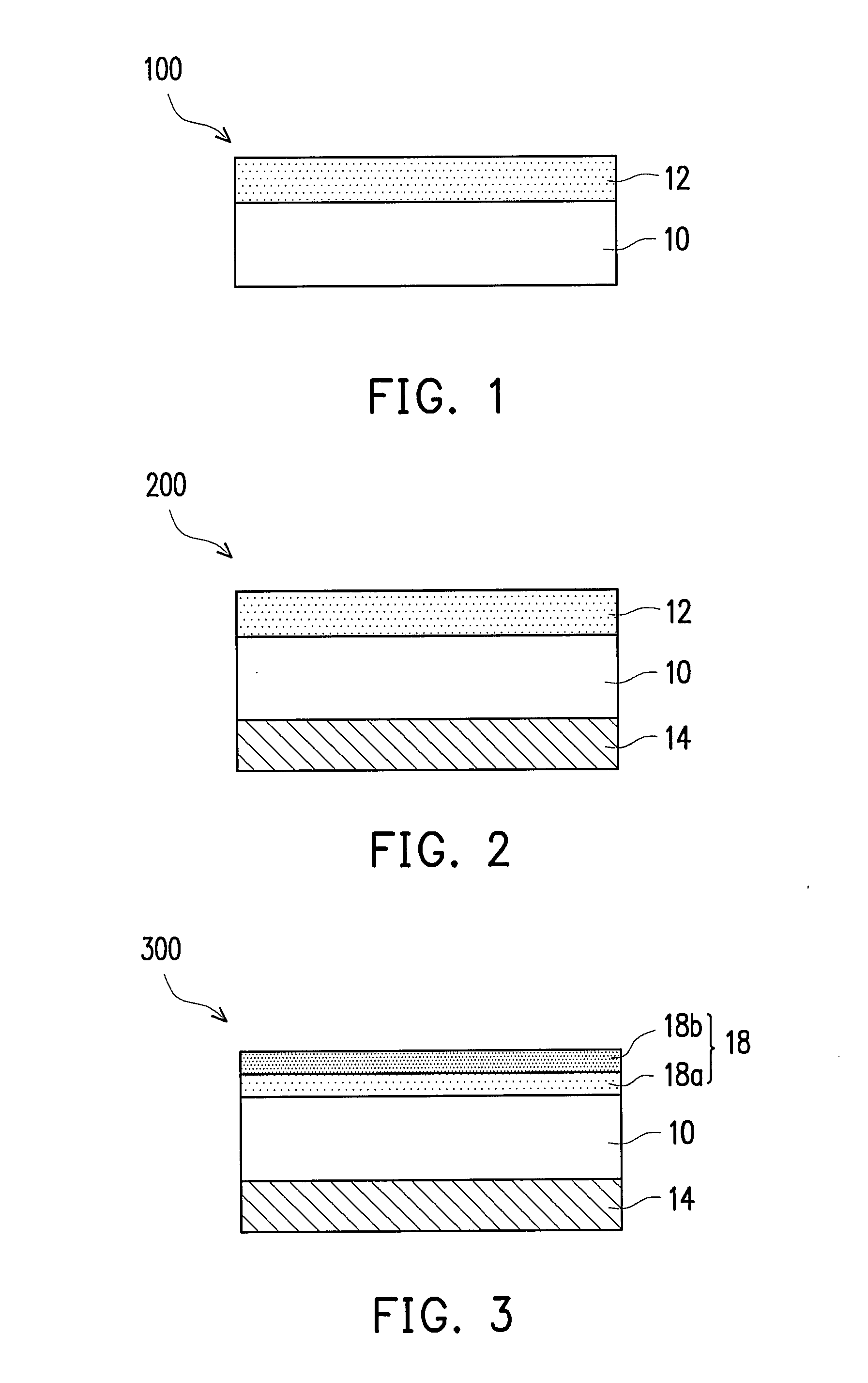
[0035]FIG. 1 is a schematic cross-sectional view of a diode adapted for an optoelectronic device according to an embodiment of the present invention.

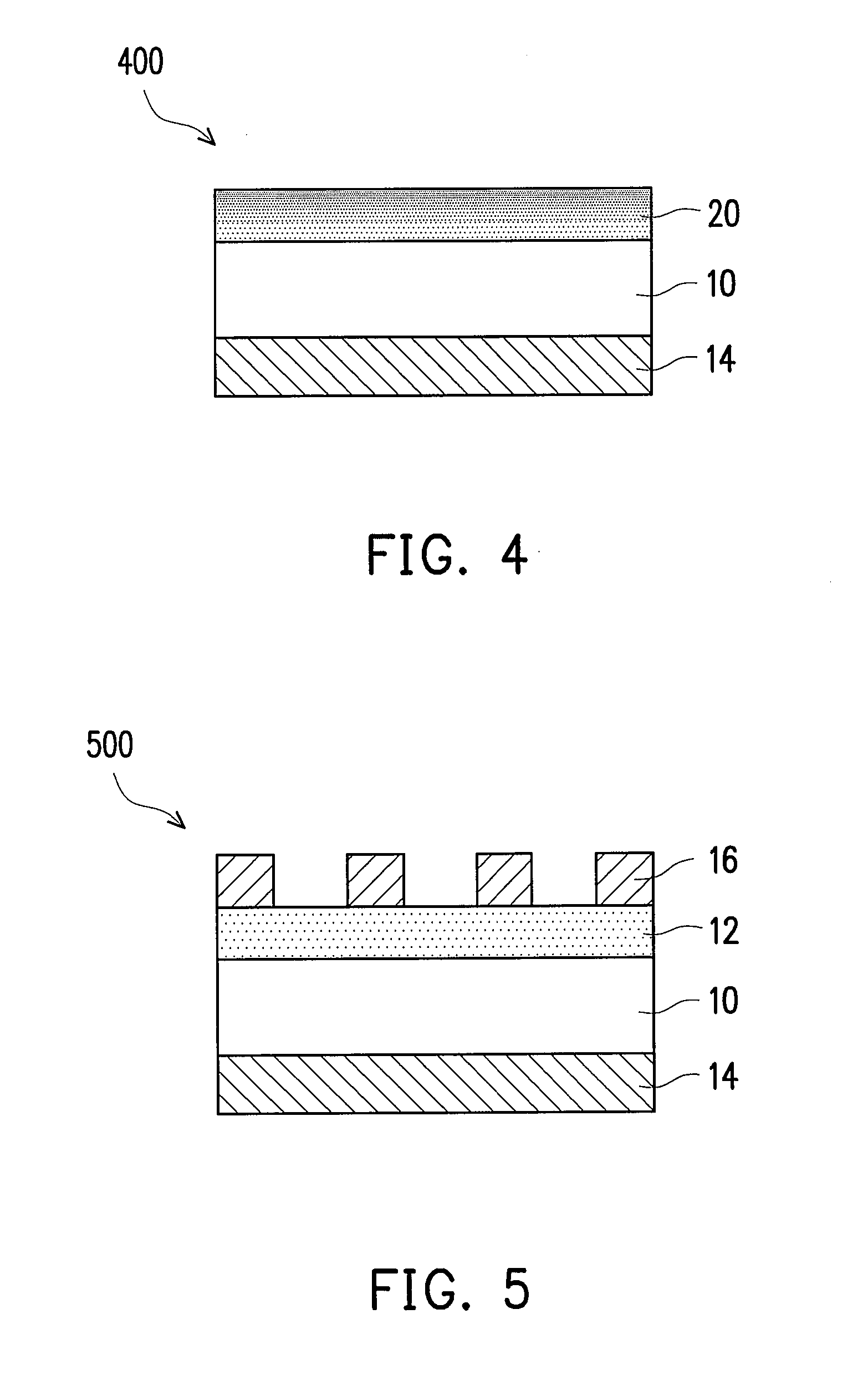
[0036]Referring to FIG. 1, a diode 100 in this embodiment comprises a P-type semiconductor substrate 10 and an N-type transparent amorphous oxide semiconductor layer 12. The P-type semiconductor substrate 10 can be a wafer or a film, for example, a P-type silicon wafer or a P-type silicon film. The P-type semiconductor substrate 10 can also be made of other P-type semiconductor materials. The N-type transparent amorphous oxide semiconductor layer 12 is disposed on the P-type semiconductor substrate. The N-type transparent amorphous oxide semiconductor layer 12 is, for example, mainly formed by ZnO, a ZnO—SnO2 mixture, or a ZnO—In2O3 mixture, and further comprises other elements. The aforesaid other elements comprise aluminum, gallium, indium, boron, yttrium, scandium, fluorine, vanadium, silicon, germanium, zirconium, hafnium, nitrogen,...


PUM


Abstract

An optoelectronic device is provided. The optoelectronic device includes a P-type semiconductor substrate, an N-type transparent amorphous oxide semiconductor (TAOS) layer located on a surface of the P-type semiconductor substrate, and a rear electrode on another surface of the P-type semiconductor substrate. The N-type TAOS layer constructs a portion of a P-N diode, and serves as a window layer and a front electrode layer.

Description

CROSS-REFERENCE TO RELATED APPLICATION[0001]This application claims the priority benefit of Taiwan application serial no. 97118368, filed on May 19, 2008. The entirety of the above-mentioned patent application is hereby incorporated by reference herein and made a part of specification.BACKGROUND OF THE INVENTION[0002]1. Field of the Invention[0003]The present invention relates to a diode adapted for an optoelectronic device and a solar cell using the diode.[0004]2. Description of Related Art[0005]A solar cell is capable of directly converting solar energy into electricity. When it comes to pollutions and the shortage of fossil fuel, the development of solar cells is brought into focus.[0006]A solar cell generates photo-electricity mainly through photo-voltaic effect. Generally, a photo-voltaic effect refers to an effect that two end electrodes of a P—N diode generate an output voltage after photons are infused to the P—N diode to generate current.[0007]In a typical solar cell, an N-...

Claims


Application Information

Patent Timeline
IPC IPC(8): H01L31/0336H01L29/861H01L29/868H01L31/06H01L31/074H01L31/10
CPCH01L31/0328H01L31/0336Y02E10/543H01L31/072H01L31/109H01L31/0376Y02E10/50
Inventor LIN, CHIUNG-WEICHEN, YI-LIANG
Owner TATUNG COMPANY
Why Eureka
Try Eureka