Exposure apparatus, exposure method, and device manufacturing method

a technology of exposure apparatus and manufacturing method, which is applied in the direction of photomechanical treatment, printing, instruments, etc., can solve the problems of inability to function normally, difficulty in measuring itself using the encoder head, etc., and achieve the effect of high accuracy

Active Publication Date: 2009-11-19
NIKON CORP
View PDF61 Cites 32 Cited by
  • Summary
  • Abstract
  • Description
  • Claims
  • Application Information

AI Technical Summary

Benefits of technology

[0012]According to this method, in the detection process, for at least one encoder head of the plurality of encoder heads, the residual state of the liquid on the photodetection surface is detected. Therefore, in the measurement process, of the plurality of encoder heads, positional information of the movable body within the predetermined plane can be measured based on an output of a predetermined number of encoder heads whose residual state of liquid on the photodetection surface is good. Accordingly, the use of the encoder head which does not function properly due to much liquid remaining on the photodetection surface can be avoided, which allows a highly accurate and a stable measurement of the positional information of the movable body.

Problems solved by technology

In such a case, measurement errors occur in an encoder head that has the liquid remaining on the photodetection surface, or in the case the residual volume is large, measurement itself using the encoder head becomes difficult, and the encoder head will not function normally.

Method used


Image

  • Exposure apparatus, exposure method, and device manufacturing method
  • Exposure apparatus, exposure method, and device manufacturing method
  • Exposure apparatus, exposure method, and device manufacturing method

Examples


first embodiment

A First Embodiment

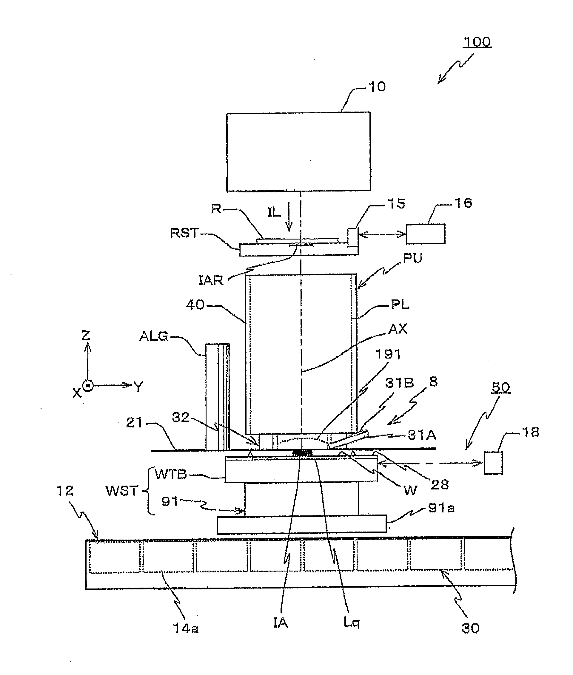
[0023]Hereinafter, a first embodiment of the present invention will be described, with reference to FIGS. 1 to 6F.

[0024]FIG. 1 shows a schematic configuration of an exposure apparatus 100 in the first embodiment. Exposure apparatus 100 is a projection exposure apparatus of the step-and-scan method, namely the so-called scanner. As it will be described later, a projection optical system PL is arranged in the embodiment, and in the description below, a direction parallel to an optical axis AX of projection optical system FL will be described as the Z-axis direction, a direction within a plane orthogonal to the Z-axis direction in which a reticle and a wafer are relatively scanned will be described as the Y-axis direction, a direction orthogonal to the Z-axis and the Y-axis will be described as the X-axis direction, and rotational (inclination) directions around the X-axis, the Y-axis, and the Z-axis will be described as θx, θy, and θz directions, respectively.

[0025]E...

second embodiment

A Second Embodiment

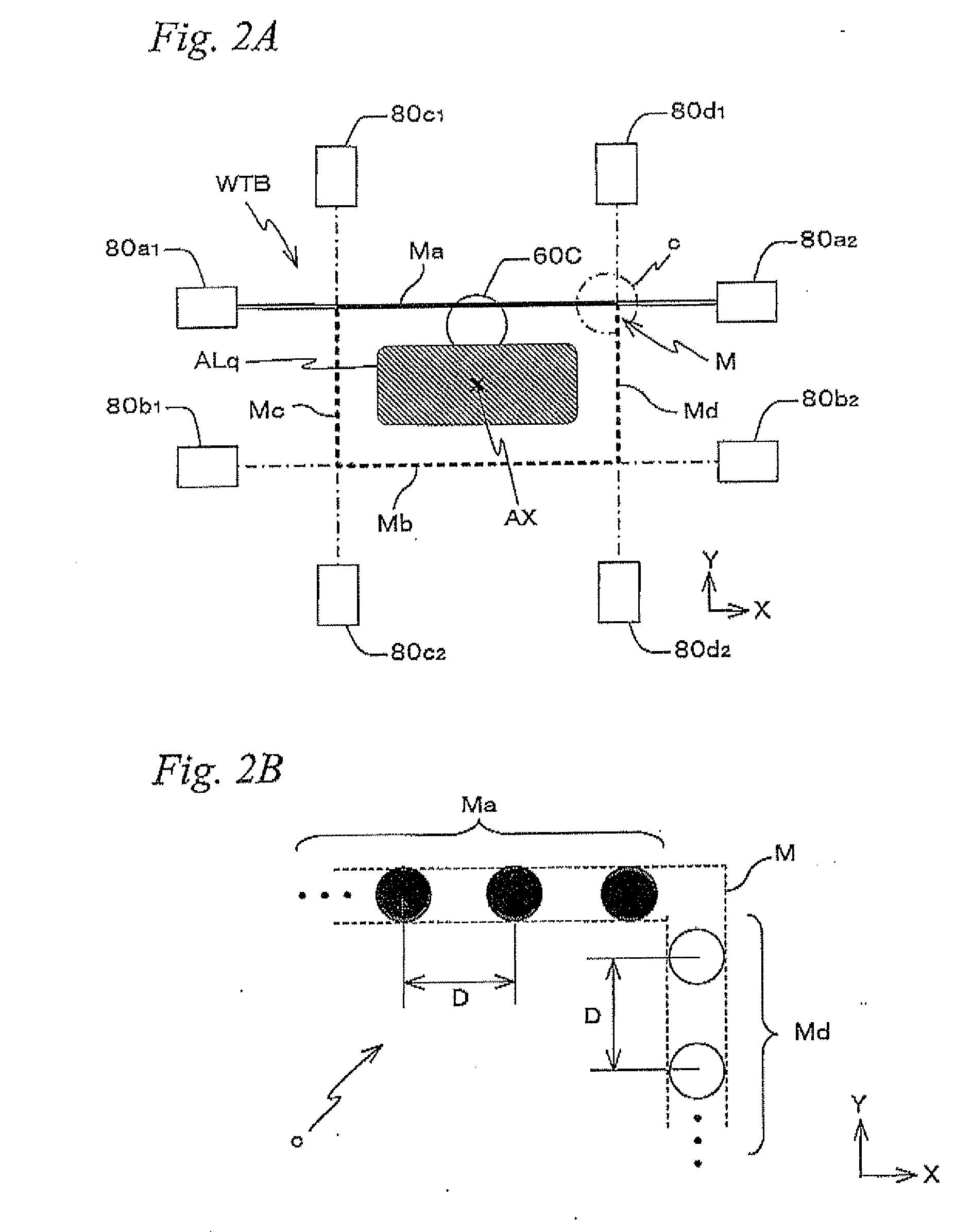
[0097]Next, a second embodiment of the present invention will be described, referring to FIG. 8. Here, the same reference numerals will be used for the same or similar sections as in the first embodiment previously described, and a detailed description thereabout will be simplified or omitted.

[0098]The exposure apparatus of the second embodiment is different from exposure apparatus 100 of the first embodiment previously described in the configuration of the encoder system which measures the positional information of wafer stage WST, especially in the placement of encoder heads on wafer stage WST and the configuration of scale plates, and as for other sections, the configuration and the like is the same. Accordingly, in the description below, the second embodiment will be described, focusing mainly on such differences. Incidentally, in the exposure apparatus of the second embodiment, liquid detecting sensors similar to liquid detecting sensor 82C (refer to FIGS. 7A...


PUM


Abstract

In an exposure apparatus of a liquid immersion exposure method, there is a case when a wafer table holding a wafer moves, a liquid immersion area formed by liquid supplied in a space between a wafer table and a projection optical system passes over a head mounted on the wafer table. Therefore, for a head over which the liquid immersion area has passed, the residual presence of the liquid is detected based on an amount of light of a reflected light received by the light receiving element which receives the reflected light from the wafer table surface. And, of a plurality of heads, positional information of the wafer table is measured, based on measurement values of a head that had no liquid remaining in the detection.

Description

CROSS-REFERENCE TO RELATED APPLICATIONS[0001]This non-provisional application claims the benefit of Provisional Application No. 61 / 071,694 filed May 13, 2008, the disclosure of which is hereby incorporated herein by reference in its entirety.BACKGROUND OF THE INVENTION[0002]1. Field of the Invention[0003]The present invention relates to exposure apparatus, exposure methods, and device manufacturing methods, and more particularly to an exposure apparatus and an exposure method used in a lithography process to manufacture microdevices such as a semiconductor device, and a device manufacturing method using the exposure method.[0004]Description of the Background Art[0005]Conventionally, in a lithography process for manufacturing electron devices (microdevices) such as semiconductor devices (such as integrated circuits) and liquid crystal display devices, exposure apparatuses such as a projection exposure apparatus by a step-and-repeat method (a so-called stepper), or a projection exposu...

Claims


Application Information

Patent Timeline
Patent Type & Authority Applications(United States)
IPC IPC(8): G03B27/52G03B27/32
CPCG03F7/70775G03F7/70341G03F7/2041H01L21/0274
Inventor KANAYA, YUHO
Owner NIKON CORP
Why Eureka
Try Eureka