This helps you quickly interpret patents by identifying the three key elements:
Problems solved by technology
Method used
Benefits of technology
Benefits of technology
[0006]Further, in the semiconductor devices whose size and thickness are demanded to be reduced, it is important to increase strength against stress from the outside (hereinafter, referred to as external stress) as well as to reduce the size and the thickness.
[0007]It is an object of an embodiment of the present invention to improve resistance to electrostatic breakdown. It is another object of an embodiment of the present invention to improve resistance to external stress as well as resistance to electrostatic breakdown even in the case of reducing the thickness and size of a semiconductor device. It is further another object of an embodiment of the present invention to suppress damage due to external stress or electrostatic discharge in the manufacture process to improve the yield.
[0010]The conductive shield diffuses and releases static electricity applied by electrostatic discharge or prevents local existence (localization) of electric charges (i.e., prevents generation of a local difference in potential on the semiconductor device), so that electrostatic breakdown of the semiconductor integrated circuit can be prevented. The conductive shield is formed so as to overlap with both surfaces of the semiconductor integrated circuit with the first insulator and the second insulator interposed therebetween.
[0017]According to another embodiment of the present invention, with the conductive shield which covers the semiconductor integrated circuit, electrostatic breakdown (malfunction of the circuit or damage of a semiconductor element) due to electrostatic discharge can be suppressed. According to another embodiment of the present invention, with a pair of insulators sandwiching the semiconductor integrated circuit, a highly reliable semiconductor device having high resistance to external stress while achieving reduction in the thickness and size can be provided. According to another embodiment of the present invention, defective shapes and deterioration in characteristics due to external stress or electrostatic discharge are prevented even in a manufacture process, so that a semiconductor device can be manufactured with a high yield.
Such a problem is a serious problem which causes reduction in reliability and productivity through a process from a manufacturing step of the semiconductor devices to the use of the semiconductor devices as a product after an inspection step, and its countermeasures are important.
Method used
Image
Click on the blue label to locate the original text in one second.
Reading with bidirectional positioning of images and text.
Examples
embodiment 1
[0040]In this embodiment, a highly reliable semiconductor device and a method for manufacturing a semiconductor device with a high yield will be described in detail with reference to FIGS. 1A to 1C, FIGS. 2A to 2C, and FIGS. 3A to 3D.
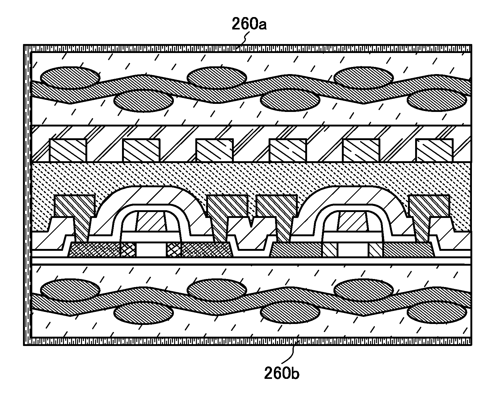
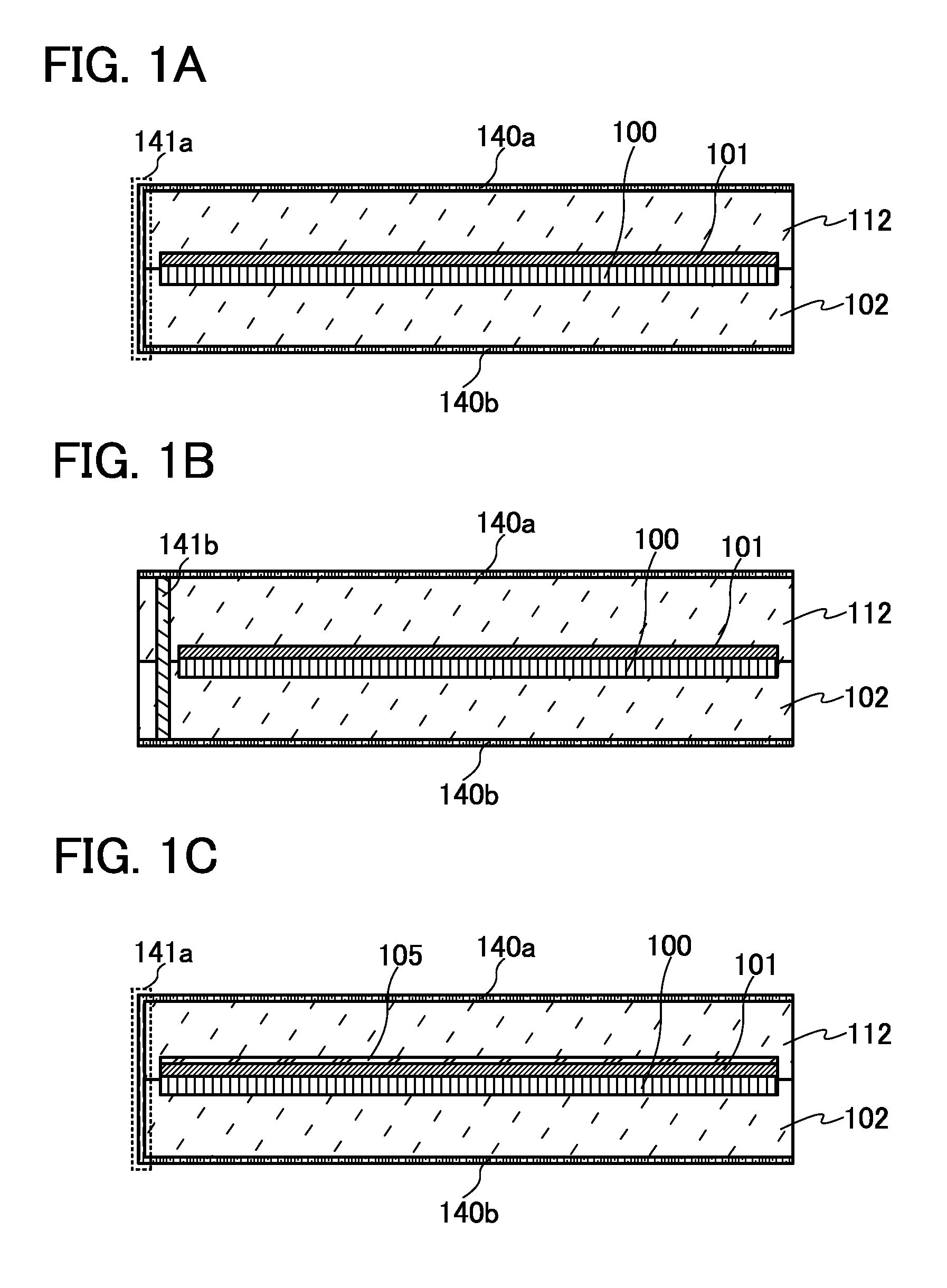
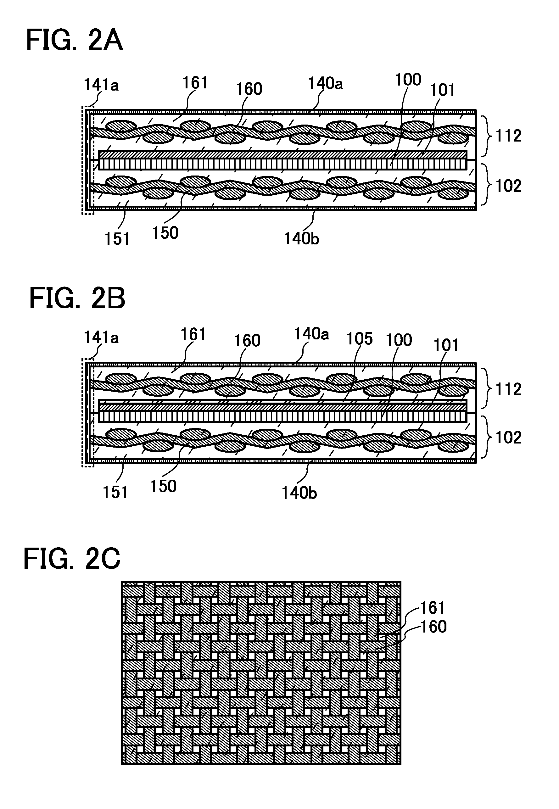
[0041]A semiconductor device of this embodiment includes a first insulator 112, a second insulator 102, a semiconductor integrated circuit 100, an antenna 101, a conductive shield 140a, and a conductive shield 140b. The first insulator 112 and the second insulator 102 are provided so as to face each other, the semiconductor integrated circuit 100 and the antenna 101 are provided between the first insulator 112 and the second insulator 102, and the conductive shields 140a and 140b are provided on surfaces (surfaces opposite to surfaces where the semiconductor integrated circuit 100 is provided) of the first insulator 112 and the second insulator 102, respectively. In addition, the conductive shield 140a provided on one surface of the first insulator 112 ...
embodiment 2
[0114]In this embodiment, another example of a semiconductor device which is different from that of the above embodiment will be described with reference to FIGS. 14A and 14B, FIGS. 15A and 15B, and FIGS. 16A to 16D. Note that the same portions or portions having a similar function as those of Embodiment 1 are denoted by the same reference numeral through different drawings in a structure of this embodiment to be described hereinafter, and repetitive description thereof is omitted.
[0115]In this embodiment, an example in which an insulator has a layered stricture is described. A semiconductor device illustrated in FIG. 14A includes the semiconductor integrated circuit 100 and the antenna 101 which are sandwiched between the first insulator 112 and the second insulator 102, a third insulator 103 provided between the semiconductor integrated circuit 100 and the second insulator 102, the conductive shield 140a provided on an outer surface of the first insulator 112, and the conductive s...
embodiment 3
[0141]In this embodiment, another example of a semiconductor device which is different from that of the above embodiment will be described with reference to FIGS. 17A to 17D. Note that the same portions or portions having a similar function as those of Embodiment 1 are denoted by the same reference numeral through different drawings in a structure of this embodiment to be described hereinafter, and repetitive description thereof is omitted.
[0142]Specifically, a case is described, in which after a conductive shield is provided for an insulator in advance, the insulator provided with the conductive shield is bonded to the semiconductor integrated circuit.
[0143]First, the antenna 101 and the semiconductor integrated circuit 100 are formed over the substrate 110 with a separation layer 111 interposed therebetween (see FIG. 17A). Note that FIG. 17A corresponds to FIG. 3A described above.
[0144]Next, after the fourth insulator 113 whose one surface is provided with the conductive shield 14...
PUM
Abstract
An object is to provide a highly reliable semiconductor device having resistance to external stress and electrostatic discharge while achieving reduction in thickness and size. Another object is to prevent defective shapes and deterioration in characteristics due to external stress or electrostatic discharge in a manufacture process to manufacture a semiconductor device with a high yield. A first insulator and a second insulator facing each other, a semiconductorintegrated circuit and an antenna provided between the first insulator and the second insulator facing each other, a conductive shield provided on one surface of the first insulator, and a conductive shield provided on one surface of the second insulator are provided. The conductive shield provided on one surface of the first insulator and the conductive shield provided on one surface of the second insulator are electrically connected.
Description
TECHNICAL FIELD[0001]The present invention relates to semiconductor devices, and in particular, semiconductor devices which transmit / receive signals to / from the outside without contact.BACKGROUND ART[0002]Semiconductor devices (such as a non-contact signalprocessing device or a semiconductor integrated circuitchip) which transmit / receive signals by wireless communication through an antenna have a problem of breakdown (electrostatic breakdown) of the semiconductor device due to electrostatic discharge (ESD). Such a problem is a serious problem which causes reduction in reliability and productivity through a process from a manufacturing step of the semiconductor devices to the use of the semiconductor devices as a product after an inspection step, and its countermeasures are important.[0003]For example, as a countermeasure against electrostatic breakdown, it is proposed to use a conductive polymer layer as for a substrate or an adhesive agent in the semiconductor device (e.g., Refer...
Claims
Application Information
Patent Timeline
Application Date:The date an application was filed.
Publication Date:The date a patent or application was officially published.
First Publication Date:The earliest publication date of a patent with the same application number.
Issue Date:Publication date of the patent grant document.
PCT Entry Date:The Entry date of PCT National Phase.
Estimated Expiry Date:The statutory expiry date of a patent right according to the Patent Law, and it is the longest term of protection that the patent right can achieve without the termination of the patent right due to other reasons(Term extension factor has been taken into account ).
Invalid Date:Actual expiry date is based on effective date or publication date of legal transaction data of invalid patent.

