Multilayer flexible wiring circuit board and its manufacturing method

Inactive Publication Date: 2005-05-03
NITTO DENKO CORP
15 Cites 7 Cited by

AI-Extracted Technical Summary

Problems solved by technology

This method has the problem that the multiple flexible wired circuit board thus produced provides increase in number of layers ...

Method used

[0087]Thereafter, the separator 39 is peeled off and removed together with the surplus solder powders 38 flowing over the first opening 34, as shown in FIG. 3(f). This can allow the solder powders 38 to be charged in the first opening 34 in a simple and reliable manner.
[0095]Also, in this process, since the third conductor layer 29 of the first single-sided substrate 30 is bonded directly to the first conductor layer 22 of the double-sided substrate 24 through the first thermosetting adhesive layer 35 without any insulating layer being interposed therebetween and also the fourth conductor layer 32 of the second single-sided base layer 33 is bonded directly to the second conductor layer 23 of the double-sided substrate 24 through the second thermosetting adhesive layer 37 without any insulating layer being interposed therebetween. This can provide a reduced thickness of the flexible wired circuit board by that extent.
[0096]Hence, the four-layered flexible wired circuit board 46 thus produced in this method can provide a higher density wiring and reduction in thickness and size.
[0097]In addition, in this method, after the solder powders 38 are charged in the first openings 34 of the first thermosetting adhesive layer 35 and the second openings 37 of the second thermosetting adhesive layer 37 under normal temperature, the first thermosetting adhesive layer 35 and the second thermosetting adhesive layer 37 are laminated on the first conductor layer 22 of the double-sided substrate 24 and the second conductor layer 23 of the same, respectively. More specifically, in the solder powder 38 charging process, the first thermosetting adhesive layer 35 and the second thermosetting adhesive layer 37 are laminated on the first conductor layer 22 and the second conductor layer 23 of the double-sided substrate 24, respectively, in the condition in which the curing of the first thermosetting adhesive layer 35 and the second thermosetting adhesive layer 37 is prevented as much as possible in the heat history for the solvent 40 to be removed from the solder paste 41 by drying. Thus, the first thermosetting adhesive layer 35 and the first conductor layer 22, and the second thermosetting adhesive layer 37 and the se...

Benefits of technology

[0020]In this conductive passage forming process, since the solder powders are charged under normal temperature and also melted by heating in the condition in which the adhesive layer is interposed between the two conductor layers, even when the adhesive layer is reactively ...

Abstract

A multilayer flexible wired circuit board that can provide high density wiring and also can provide reduction in thickness and size, and a producing method thereof. A four-layered flexible wired circuit board is produced by preparing a double-sided substrate in which a first conductor layer and a second conductor layer are laminated on both sides of a first insulating layer; preparing a first single-sided substrate in which a third conductor layer is laminated on one surface of a second insulating layer and a second single-sided substrate in which a fourth conductor layer is laminated on one surface of a third insulating layer; bonding the first conductor layer and the third conductor layer to each other through a first thermosetting adhesive layer; and bonding the second conductor layer and the fourth conductor layer to each other through a second thermosetting adhesive layer.

Application Domain

Printed circuit aspectsLamination +8

Technology Topic

EngineeringElectrical conductor +1

Image

  • Multilayer flexible wiring circuit board and its manufacturing method
  • Multilayer flexible wiring circuit board and its manufacturing method
  • Multilayer flexible wiring circuit board and its manufacturing method

Examples

  • Experimental program(2)

Example

Example 1
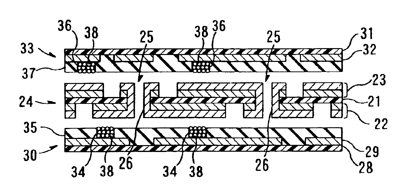
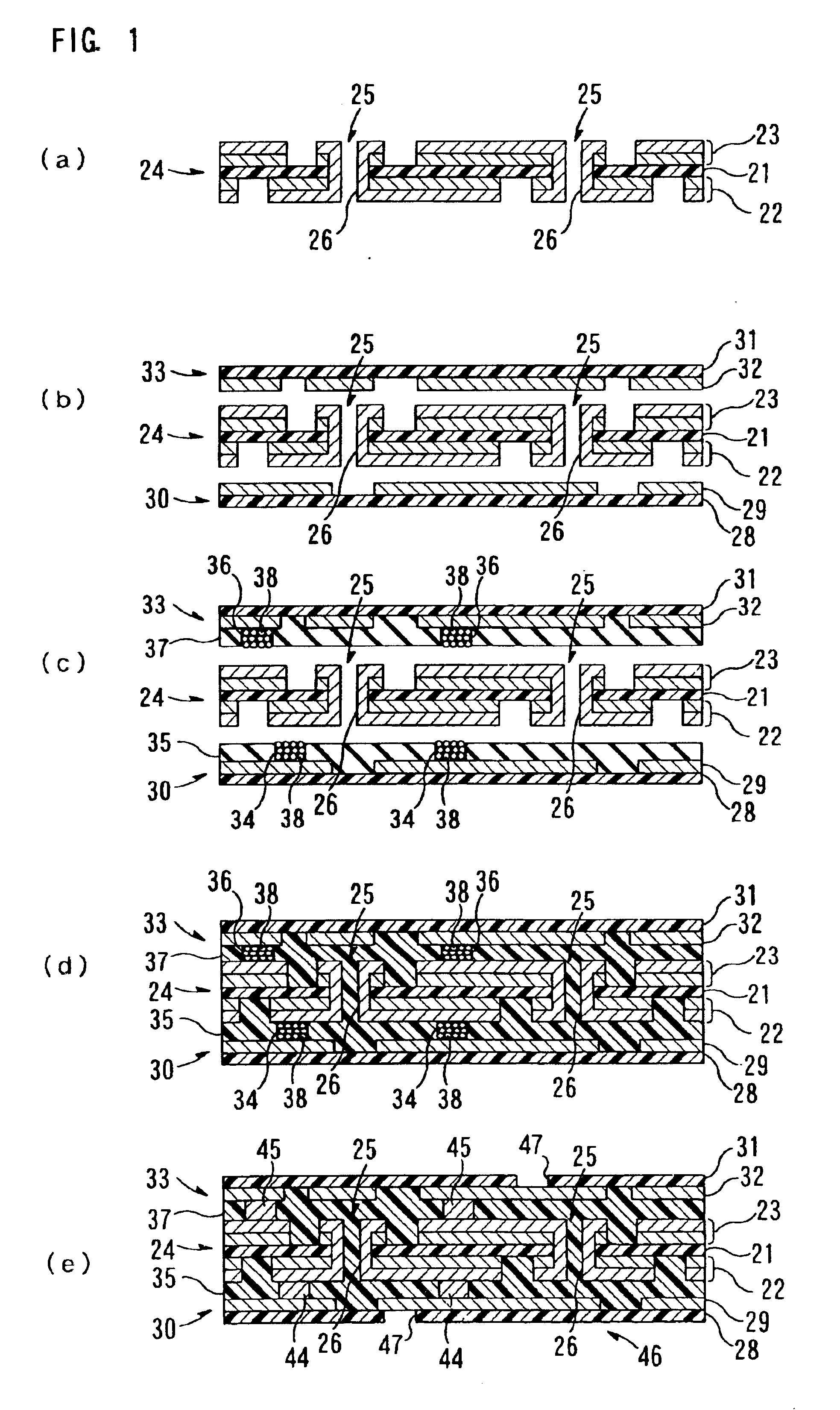
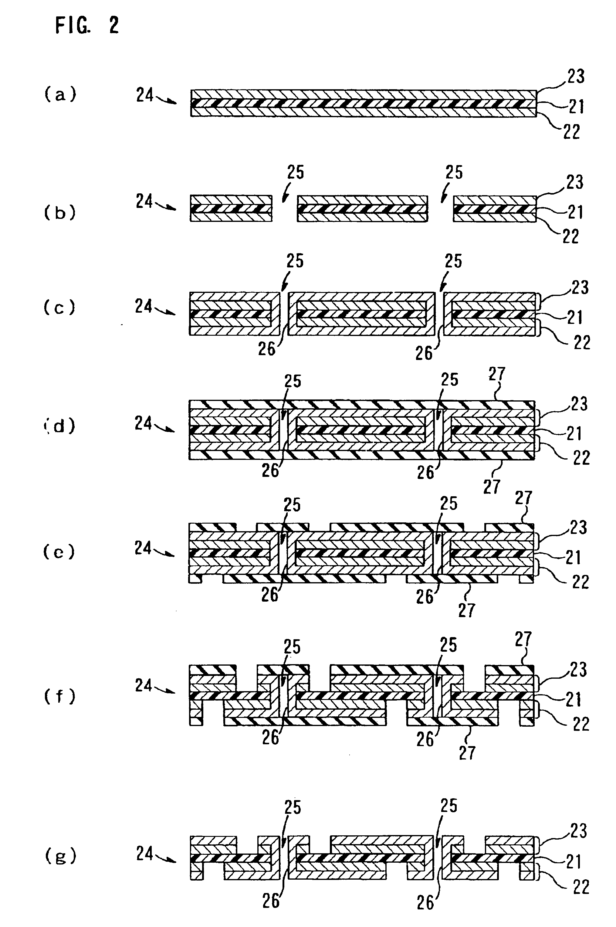
[0101]The double-sided substrate, in which the first conductor layer and the second conductor layer, each comprising a copper foil having thickness of 18 μm, are laminated on both sides of the first insulating layer comprising polyimide resin having thickness of 13 μm, respectively, was prepared (See FIG. 2(a)).
[0102]Then, after through holes having a diameter of 100 μmφ was formed in the double-sided substrate at specified positions thereof by drilling (FIG. 2(b)), the through holes were plated with copper to form the through-hole plated layers having thickness of 18 μm (FIG. 2(c)).
[0103]Sequentially, photoresists comprising dry film resist were laminated on the first conductor layer and the second conductor layer, respectively (See FIG. 2(d)). Then, the photoresists were exposed to light through photomasks corresponding to their specific patterns and then developed, to form the photoresists in specific resist patterns (See FIG. 2(e)).
[0104]Then, the first conductor layer and the second conductor layer were each etched by using ferric (II) chloride solution (See FIG. 2(f)) and, thereafter, the photoresists were peeled off, to form the first conductor layer and the second conductor layer in their respective specific wired circuit patterns (See FIG. 2(g)).
[0105]The first single-sided substrate in which the third conductor layer comprising a copper foil having thickness of 18 μm was formed on one surface of the second insulating layer comprising polyimide resin having thickness of 13 μm was prepared separately. Then, after the third conductor layer was formed in a specific wired circuit pattern by the subtractive process (See FIG. 3(a)), the first thermosetting adhesive layer comprising an adhesive sheet of acrylic adhesive having thickness of 50 μm was laminated on (temporarily bonded to) the third conductor layer by using a vacuum press at 50° C. under pressure of 1.5 MPa, the first openings having the diameter of 150 μmφ were formed in specified areas of the first thermosetting adhesive layer (where the first conductor layer and the third conductor layer are connected with each other) by using the YAG laser (See FIG. 3(b)).
[0106]Then, after the metal mask formed in a specific pattern corresponding to the first openings was set in place on the first thermosetting adhesive layer, the solder paste was printed on the first thermosetting adhesive layer through the metal mask (See FIG. 3(c)). The solder paste available from NIHON GENMA MFG. CO. LTD. was used in which the solder powders comprising Sn/Ag having an average particle diameter of 20 μm, alcohols solvent, and amide resin were mixed in the ratio of 50:49:1 by volume.
[0107]Then, after the solvent was dried and removed by heating at 160° C. for 5 minutes (FIG. 3(d)), the solder powders were pressed under normal temperature at 5 MPa for 5 minutes (FIG. 3(e)) and then the surplus solder powders were removed (See FIG. 3(f)).
[0108]Further, the second single-sided substrate in which the fourth conductor layer comprising a copper foil having thickness of 18 μm was formed on one surface of the third insulating layer comprising polyimide resin having thickness of 13 μm was prepared. Then, after the fourth conductor layer was formed in a specific wired circuit pattern by the subtractive process, the second thermosetting adhesive layer comprising an adhesive sheet of acrylic adhesive having thickness of 50 μm was laminated on (temporarily bonded to) the fourth conductor layer by using the vacuum press at 50° C. under pressure of 1.5 MPa, the second openings having the diameter of 150 μmφ (were formed in specified areas of the second thermosetting adhesive layer (where the second conductor layer and the fourth conductor layer are connected with each other) by using the YAG laser.
[0109]Then, after the metal mask formed in a specific pattern corresponding to the second openings was set in place on the second thermosetting adhesive layer, the solder paste was printed on the second thermosetting adhesive layer through the metal mask. The solder paste available from NIHON GENMA MFG. CO. LTD. was used in which the solder powders comprising Sn/Ag having an average particle diameter of 20 μm, alcohols solvent, and amide resin were mixed in the ratio of 50:49:1 by volume.
[0110]Then, after the solvent was dried and removed by heating at 160° C. for 5 minutes, the solder powders were pressed under normal temperature at 5 MPa for 5 minutes and then the surplus solder powders were removed.
[0111]Then, the first thermosetting adhesive layer laminated on the first single-sided substrate was positioned on the first conductor layer of the double-sided substrate to be in alignment therewith and was put into close contact therewith. Also, the second thermosetting adhesive layer laminated on the second single-sided substrate was positioned on the second conductor layer of the double-sided substrate to be in alignment therewith and was put into close contact therewith. Thereafter, the first thermosetting adhesive layer and the second thermosetting adhesive layer were heated at 200° C. under pressure of 5 MPa for 30 minutes, so that the first single-sided substrate was laminated on the first conductor layer of the double-sided substrate and the second single-sided substrate was laminated on the second conductor layer of the double-sided substrate (See FIG. 1(d)).
[0112]Thereafter, the solder powders were melted by heating at 230° C. under pressure of 5 MPa for 3 minutes, to form the first conductive passage for electrically connecting between the first conductor layer and the third conductor layer which were bonded to each other through the first thermosetting adhesive layer and the second conductive passage for electrically connecting between the second conductor layer and the fourth conductor layer which were bonded to each other through the second thermosetting adhesive layer. After these processes, the four-layered flexible wired circuit board was produced (See FIG. 1(d)). The second insulating layer and the third insulating layer of the four-layered flexible wired circuit board thus obtained were bored at specific areas thereof by using the YAG laser, to form the terminal openings.
[0113]The overall thickness of the four-layered flexible wire circuit board thus obtained was 193 μm.

Example

Comparative Example 1
[0114]The double-sided substrate, in which the first conductor layer and the second conductor layer, each comprising a copper foil having thickness of 18 μm, were laminated on both sides of the first insulating layer comprising polyimide resin having thickness of 13 μm, respectively, was prepared, first (See FIG. 4(a)). Then, the second insulating layer and the third insulating layer, each comprising polyimide resin having thickness of 13 μm, were laminated on the first conductor layer and the second conductor layer of the double-sided substrate through the first adhesive layer and the second adhesive layer comprising acrylic adhesive having thickness of 25 μm, respectively (See FIG. 4(b)).
[0115]The first single-sided substrate, in which the third conductor layer comprising a copper foil having thickness of 18 μm was laminated on the four insulating layer comprising polyimide resin having thickness of 13 μm, and the second single-sided substrate, in which the fourth conductor layer comprising a copper foil having thickness of 18 μm was laminated on the fifth insulating layer comprising polyimide resin having thickness of 13 μm, were prepared separately (See FIG. 4(c)). Then, the first cover insulating layer comprising polyimide resin having thickness of 13 μm was laminated on the third conductor layer of the first single-sided substrate through the third adhesive layer comprising acrylic adhesive having thickness of 15 μm, and the second cover insulating layer comprising polyimide resin having thickness of 13 μm was laminated on the fourth conductor layer of the second single-sided substrate through the fourth adhesive layer comprising acrylic adhesive having thickness of 15 μm (See FIG. 4(d)).
[0116]Then, the fourth insulating layer of the first single-sided substrate was laminated on the second insulating layer laminated on the double-sided substrate through the fifth adhesive layer comprising acrylic adhesive having thickness of 25 μm, and the fifth insulating layer of the second single-sided substrate was laminated on the third insulating layer laminated on the double-sided substrate through the sixth adhesive layer comprising acrylic adhesive having thickness of 25 μm. After these processes, the four-layered flexible wired circuit board was obtained (See FIG. 1(e)). The overall thickness of the four-layered flexible wired circuit board thus obtained was 293 μm.
[0117]While the illustrative embodiment and example of the present invention are provided in the above description, such is for illustrative purpose only and it is not to be construed restrictively. Modification and variation of the present invention that will be obvious to those skilled in the art is to be covered by the following claims.
Capabilities of Exploitation in Industry
[0118]As mentioned above, a multilayer flexible wired circuit board of the present invention produced by a method of producing the multilayer flexible wired circuit board of the present invention is effectively usable as a multilayer flexible wired circuit board which is required for high density wiring and reduction in thickness and size.

PUM

PropertyMeasurementUnit
Temperature
Thickness
Size

Description & Claims & Application Information

We can also present the details of the Description, Claims and Application information to help users get a comprehensive understanding of the technical details of the patent, such as background art, summary of invention, brief description of drawings, description of embodiments, and other original content. On the other hand, users can also determine the specific scope of protection of the technology through the list of claims; as well as understand the changes in the life cycle of the technology with the presentation of the patent timeline. Login to view more.

Similar technology patents

Adhesive sheet

InactiveUS20090291300A1moderate adhesive propertyincrease adhesion strength
Owner:LINTEC CORP

Wired circuit board

ActiveUS20060199402A1transmission loss be reducesufficient adhesive strength
Owner:NITTO DENKO CORP

Adhesive patch containing bisoprolol

InactiveUS20130006203A1reduce opportunitysufficient adhesive strength
Owner:NITTO DENKO CORP +1

Sealing member for light guide plate and planar light source device or lighting device using the same

InactiveUS20200363582A1high smoothnesssufficient adhesive strength
Owner:TOMOEGAWA CO LTD

Inkjet print head

ActiveUS20200290353A1sufficient adhesive strength
Owner:CANON KK

Loudspeaker

ActiveUS20050041830A1increase adhesion strength
Owner:PANASONIC CORP

Classification and recommendation of technical efficacy words

  • increase adhesion strength
  • sufficient adhesive strength

Loudspeaker

ActiveUS20050041830A1increase adhesion strength
Owner:PANASONIC CORP

Adhesive sheet

InactiveUS20090291300A1moderate adhesive propertyincrease adhesion strength
Owner:LINTEC CORP

Wired circuit board

ActiveUS20060199402A1transmission loss be reducesufficient adhesive strength
Owner:NITTO DENKO CORP

Adhesive patch containing bisoprolol

InactiveUS20130006203A1reduce opportunitysufficient adhesive strength
Owner:NITTO DENKO CORP +1

Inkjet print head

ActiveUS20200290353A1sufficient adhesive strength
Owner:CANON KK

Sealing member for light guide plate and planar light source device or lighting device using the same

InactiveUS20200363582A1high smoothnesssufficient adhesive strength
Owner:TOMOEGAWA CO LTD
Why Eureka
Try Eureka