Multi-row wiring member for semiconductor device and method for manufacturing the same

Active Publication Date: 2019-06-04
CHANG WAH TECH
View PDF22 Cites 2 Cited by
  • Summary
  • Abstract
  • Description
  • Claims
  • Application Information

AI Technical Summary

Benefits of technology

[0013]The inventors of the present application, upon repeated trial and error at the stage before introducing the present invention, have devised a wiring member for semiconductor device that enables manufacturing of a highly-reliable resin-sealed semiconductor device through a reduced number of steps and a manufacturing method for the same wiring member; the wiring member enables reduction in thickness and size of the semiconductor device, improves adhesion between a plating film that forms terminal portions and a resin, achieves uniform height of a surface of the internal-terminal-side plating layer on which the semiconductor element is to be mounted and internal terminal portions to be electrically connected with the semiconductor element, eliminates, in the manufacturing process for the semiconductor device, the step of removing the metal sheet by etching and the step of forming openings that uncover external terminal portions alone, and moderating a warpage of the sealing resin as cured.

Problems solved by technology

As a result of further study and consideration, the inventors of the present application have found that this prototypal wiring member for semiconductor device and the method for manufacturing the same as devised involved problems to be improved for mass-production of semiconductor devices.

Method used


Image

  • Multi-row wiring member for semiconductor device and method for manufacturing the same
  • Multi-row wiring member for semiconductor device and method for manufacturing the same
  • Multi-row wiring member for semiconductor device and method for manufacturing the same

Examples


first embodiment

Mode

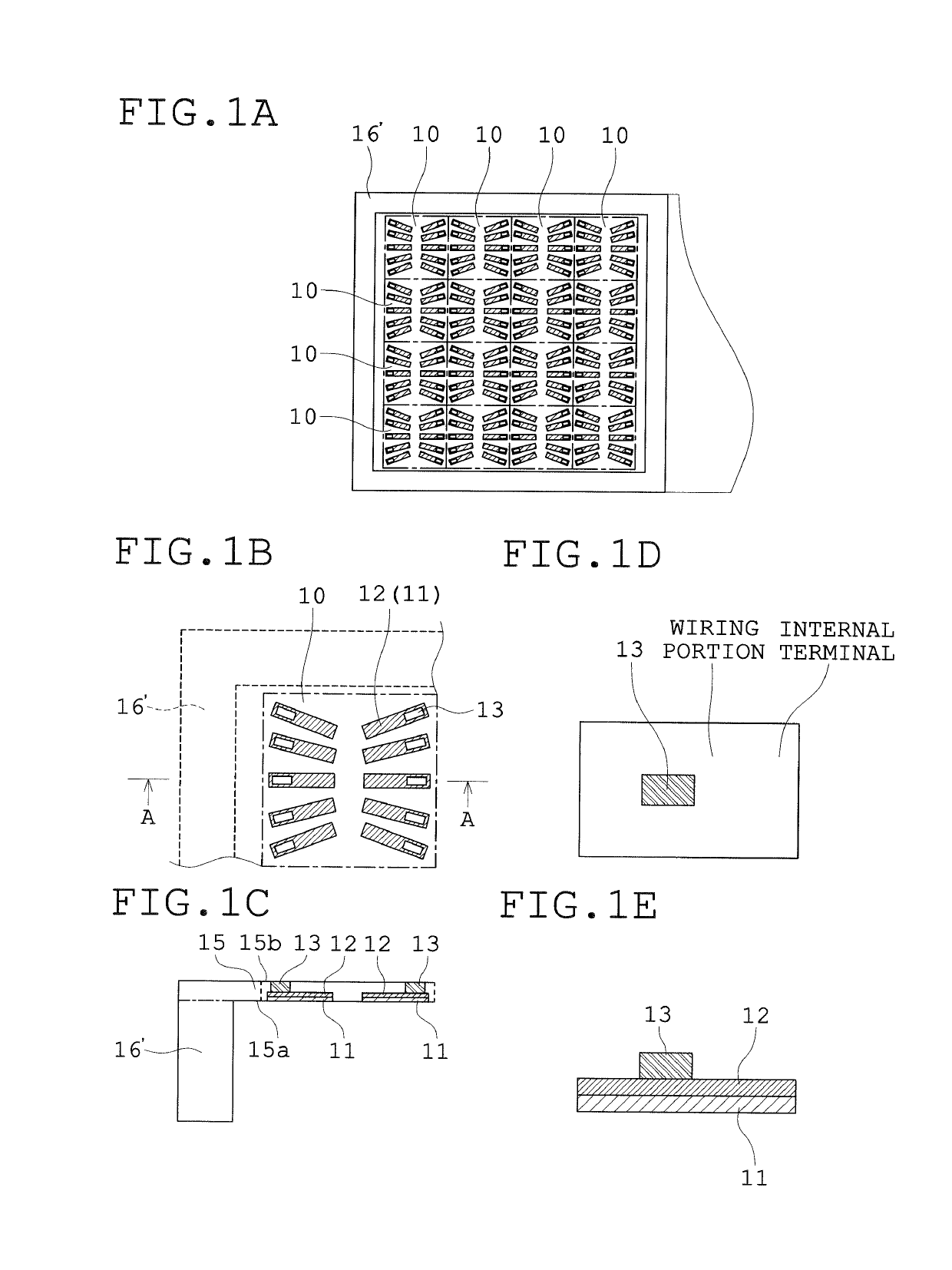
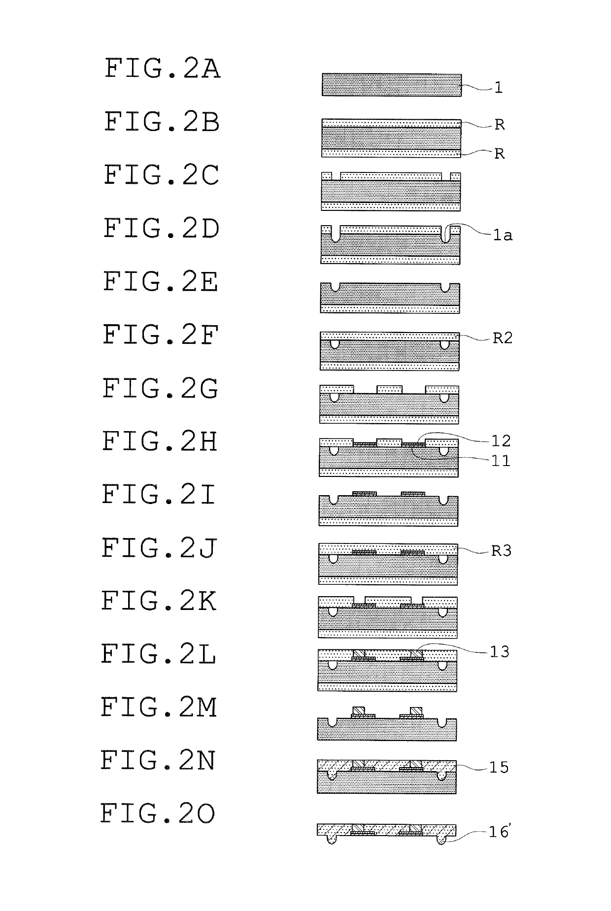
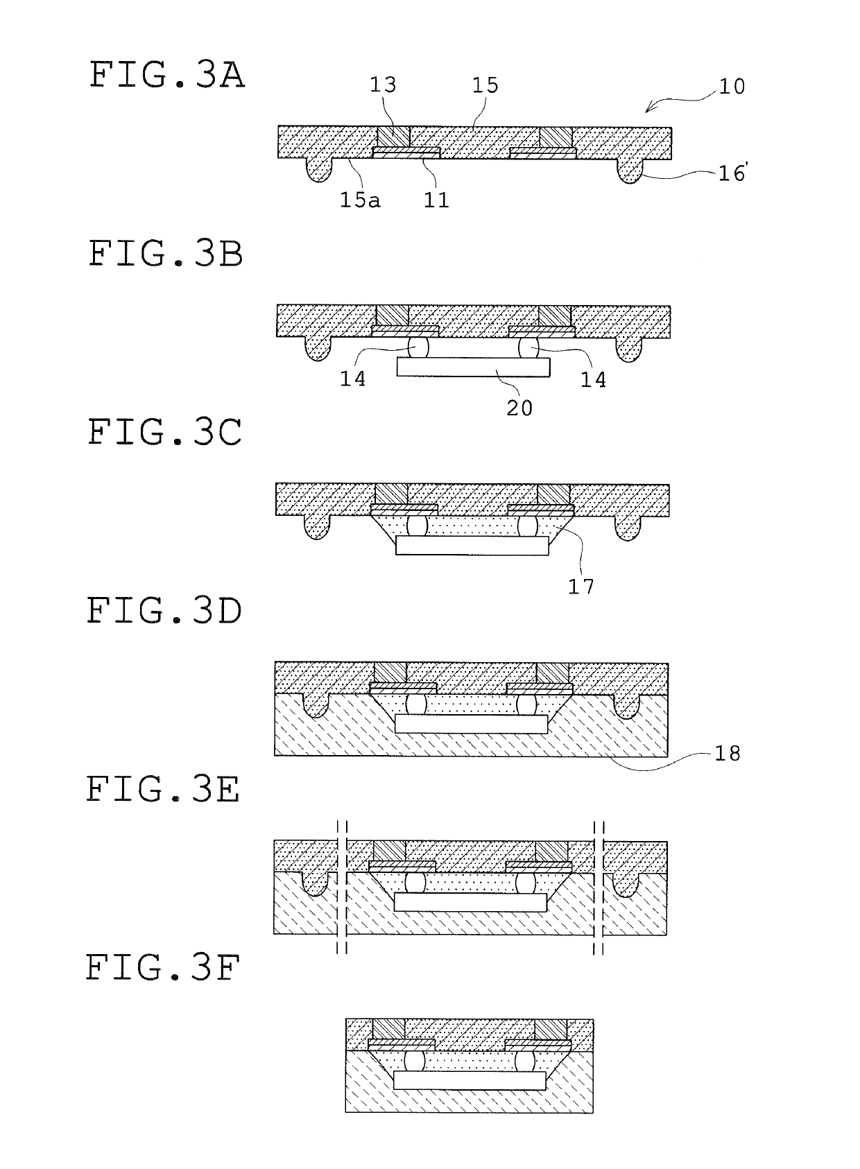
[0065]FIGS. 1A-1E are diagrams that show the configuration of the multi-row wiring member for semiconductor device according to the first embodiment mode of the present invention, where FIG. 1A is a plan view as viewed from the external-terminal side, FIG. 1B is an enlarged view of a part of FIG. 1A, FIG. 1C is a sectional view taken along A-A of FIG. 1B, FIG. 1D is a plan view that shows one example of a laminated piece of plating layers forming an internal terminal, a wiring portion and an external terminal in an individual wiring member for a semiconductor device, and FIG. 1E is a sectional view of FIG. 1D. FIGS. 2A-2O are explanatory diagrams that show the manufacturing process for the multi-row wiring member for semiconductor device shown in FIGS. 1A-1E. FIGS. 3A-3F are explanatory diagrams that show one example of the manufacturing process for a resin-sealed semiconductor device using the multi-row wiring member for semiconductor device of the first embodiment mode manufac...

embodied example

[0111]Next, description will be made of an embodied example of the multi-row wiring member for semiconductor device and the manufacturing method therefor.

[0112]Although pre-treatment and post-treatment including chemical cleaning, aqueous washing and the like were carried out in each step, they are common treatment and thus description is omitted.

[0113]First, a copper material having a thickness of 0.15 mm, which is for the use as a lead frame material also, was prepared as a metal sheet (See FIG. 2A).

[0114]In the step of forming a first resist mask, dry film resist R having a thickness of 25 μm was made to laminate both surfaces of the metal sheet (see FIG. 2B).

[0115]Then, the dry film resist R on the front surface side was exposed and developed upon use of a glass mask carrying a pattern for forming an opening at a site that is to be a margin around an aggregate of wiring members for semiconductor devices, to form a first resist mask having an opening at a site that is to be a mar...


PUM


Abstract

A multi-row wiring member for semiconductor device configured of a plurality of wiring members arrayed in a matrix includes a resin layer, a first plating layer forming internal terminals, a plating layer forming wiring portions and a second plating layer forming external terminals. The first plating layer is formed in the resin layer with lower faces thereof uncovered in the bottom surface of the resin layer. The plating layer forming wiring portions is formed on the first plating layer in the resin layer. The second plating layer is formed on partial areas within areas of the plating layer forming wiring portions, with upper faces thereof being uncovered on a top-surface side of the resin layer. On a bottom-surface side of the resin layer, a resin frame is integrally formed with the resin layer at the margin around an aggregate of individual wiring members for semiconductor devices arrayed in a matrix.

Description

CROSS-REFERENCE TO RELATED PATENT APPLICATIONS[0001]This application is a continuation of PCT International Application No. PCT / JP2017 / 003031, filed on Jan. 27, 2017, and claims the benefit of Japanese Patent Application No. 2016-101948 filed in Japan on May 20, 2016. The contents of PCT International Application No. PCT / JP2017 / 003031 and Japanese Patent Application No. 2016-101948 are incorporated herein by reference.BACKGROUND OF THE INVENTION[0002]1) Field of the Invention[0003]The present invention relates to a multi-row wiring member for semiconductor device for achieving flip-chip mounting of semiconductor elements thereon and a method for manufacturing the same.[0004]2) Description of Related Art[0005]Conventionally, of substrates for semiconductor devices, there are those of a type intended to complete a semiconductor device by peeling off a base material thereof after mounting a semiconductor element thereon and sealing the entirety with a resin, as described in Japanese Pa...

Claims


Application Information

Patent Timeline
Patent Type & Authority Patents(United States)
IPC IPC(8): H05K1/18H01L23/50H01L21/48H05K3/30H01L23/498H01L23/00
CPCH01L23/49822H01L21/4857H01L23/50H05K3/303H05K1/18H01L2224/16227H01L24/16H01L2924/181H01L2224/16225H01L2224/48091H01L2224/73204H01L2224/73265H01L2224/92125H01L2924/00014H01L23/49827H01L23/49838H01L21/486H01L24/13H01L24/32H01L24/81H01L24/92H01L24/97H01L2221/68345H01L2224/13101H01L2224/32225H01L2224/81411H01L2224/81439H01L2224/81444H01L2224/81447H01L2224/81455H01L2224/81464H01L2924/15173H01L2924/10161H01L21/6835H01L21/561H01L2924/00012H01L2224/45099H01L2924/014H01L2224/29099H01L23/31H01L23/525H01L23/528H01L24/43H01L24/45H05K1/11H05K3/00H05K1/02H05K3/40
Inventor HISHIKI, KAORUIIDANI, ICHINORI
Owner CHANG WAH TECH
Why Eureka
Try Eureka