Process management method and process management data for semiconductor device

a technology of process management and semiconductor devices, applied in semiconductor/solid-state device testing/measurement, stochastic cad, instruments, etc., can solve problems such as affecting circuit delay, actual product malfunction, and increase the number of circuit design modification times

Inactive Publication Date: 2009-11-26
RENESAS ELECTRONICS CORP
View PDF5 Cites 3 Cited by
  • Summary
  • Abstract
  • Description
  • Claims
  • Application Information

AI Technical Summary

Problems solved by technology

Such manufacturing variability of the interconnect structure affects delay in a circuit.
Thus, even if a designed circuit passes delay verification on a computer, an actual product may malfunction since the manufacturing variability occurs.
As the condition becomes stricter, the delay verification is more likely to result in fail and thus the number of circuit design modification times increases.
This causes increase in a design time required for the circuit design.

Method used


Image

  • Process management method and process management data for semiconductor device
  • Process management method and process management data for semiconductor device
  • Process management method and process management data for semiconductor device

Examples


Embodiment Construction

[0037]The invention will be now described herein with reference to illustrative embodiments. Those skilled in the art will recognize that many alternative embodiments can be accomplished using the teachings of the present invention and that the invention is not limited to the embodiments illustrated for explanatory purposed.

[0038]In the present embodiment, a technique of managing manufacturing variability of an interconnection included in a semiconductor device is provided.

[0039]1. Overview

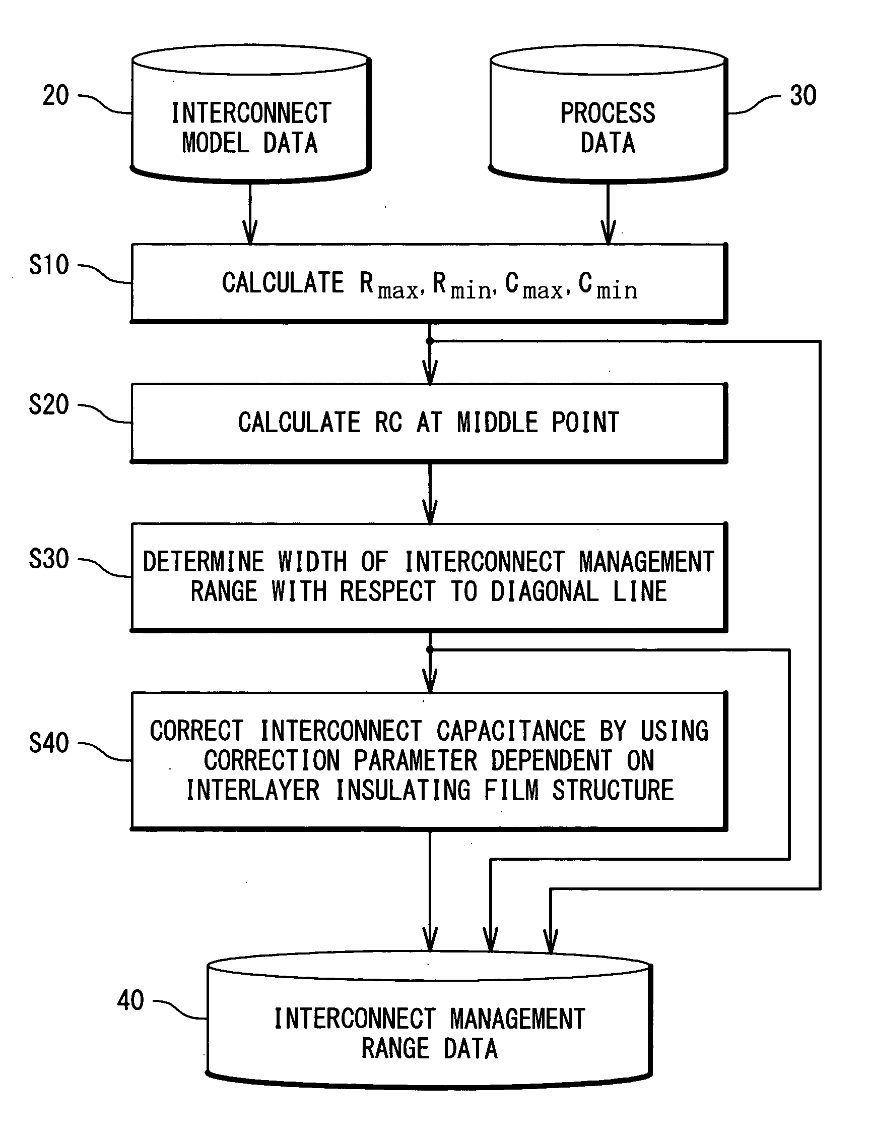
[0040]With speeding up and increasing miniaturization of a semiconductor device, management of manufacturing variability of an interconnection becomes more and more important. To that end, it is necessary in a development stage to previously estimate manufacturing variability of interconnect characteristics such as interconnect resistance and interconnect capacitance based on process specification and an interconnect model. The interconnect characteristics such as interconnect resistance and inter...


PUM


Abstract

A process management method for managing manufacturing variability of an interconnection included in a semiconductor device is provided. The process management method includes: calculating interconnect resistance and interconnect capacitance regarding an interconnection included in the semiconductor device, under a condition that manufacturing variability of a width and a thickness of the interconnection is expressed by points on a predetermined circle of equal probability of a joint probability density function; and defining, based on the calculated interconnect resistance and interconnect capacitance, a variation range of interconnect resistance and interconnect capacitance caused by manufacturing variability. The variation range is defined two-dimensionally in a coordinate system where a first axis represents interconnect resistance and a second axis represents interconnect capacitance.

Description

INCORPORATION BY REFERENCE[0001]This application is based upon and claims the benefit of priority from Japanese patent application No. 2008-133868, filed on May 22, 2008, the disclosure of which is incorporated herein in its entirety by reference.BACKGROUND OF THE INVENTION[0002]1. Field of the Invention[0003]The present invention relates to a technique of managing manufacturing variability of an interconnection and a device included in a semiconductor device.[0004]2. Description of Related Art[0005]In a manufacturing process of a semiconductor device, an interconnect structure may not be manufactured as expected. That is, physical parameters such as a width and a thickness of an interconnection, a thickness of an interlayer insulating film and the like may vary from their desired design values. Such manufacturing variability of the interconnect structure affects delay in a circuit. Thus, even if a designed circuit passes delay verification on a computer, an actual product may malfu...

Claims


Application Information

Patent Timeline
Patent Type & Authority Applications(United States)
IPC IPC(8): H01L21/66G06F19/00G06F17/50H01L21/3205H01L21/768H01L21/82H01L23/522
CPCG06F2217/10H01L22/14H01L22/20H01L2924/0002H01L2924/00G06F2111/08
Inventor ASAI, YOSHIHIKO
Owner RENESAS ELECTRONICS CORP
Why Eureka
Try Eureka