Sensitivity analysis system and sensitivity analysis program

a sensitivity analysis and program technology, applied in the field of semiconductor device design technique, can solve problems such as affecting circuit design delay, actual product malfunction, and increase the number of circuit design modification tim

Active Publication Date:
View PDF10 Cites 3 Cited by
  • Summary
  • Abstract
  • Description
  • Claims
  • Application Information

AI Technical Summary

Benefits of technology

[0013]According to the present invention, it is possible to analyze influence of the manufacturing variability of the contact structure on the parasitic capacitance.

Problems solved by technology

Such manufacturing variability affects delay in a circuit.
Thus, even if a designed circuit passes timing verification on a computer, an actual product may malfunction since the manufacturing variability occurs.
As the condition becomes stricter, the timing verification is more likely to result in fail and thus the number of circuit design modification times increases.

Method used


Image

  • Sensitivity analysis system and sensitivity analysis program
  • Sensitivity analysis system and sensitivity analysis program
  • Sensitivity analysis system and sensitivity analysis program

Examples


Embodiment Construction

[0039]The invention will be now described herein with reference to illustrative embodiments. Those skilled in the art will recognize that many alternative embodiments can be accomplished using the teachings of the present invention and that the invention is not limited to the embodiments illustrated for explanatory purposed.

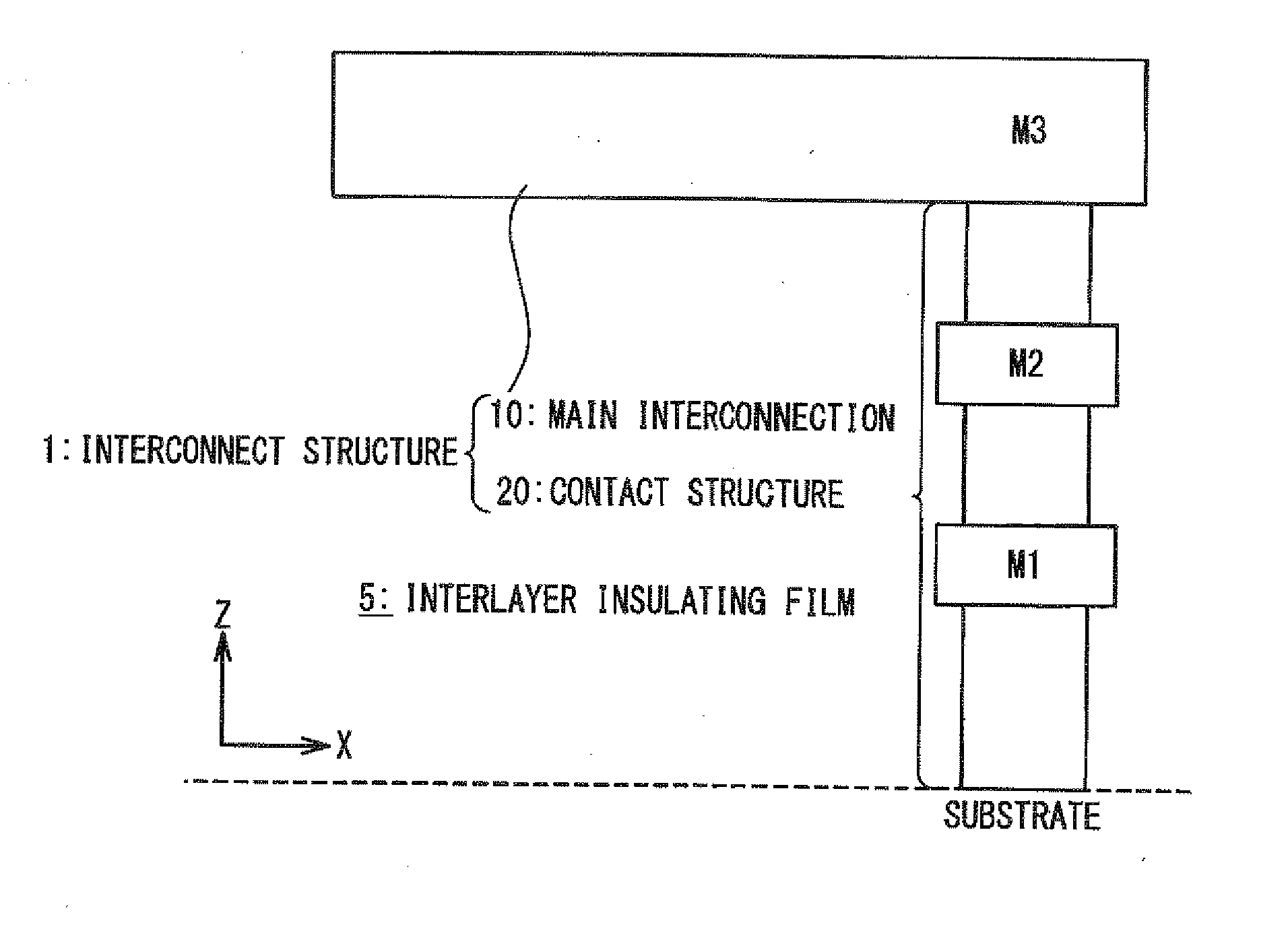
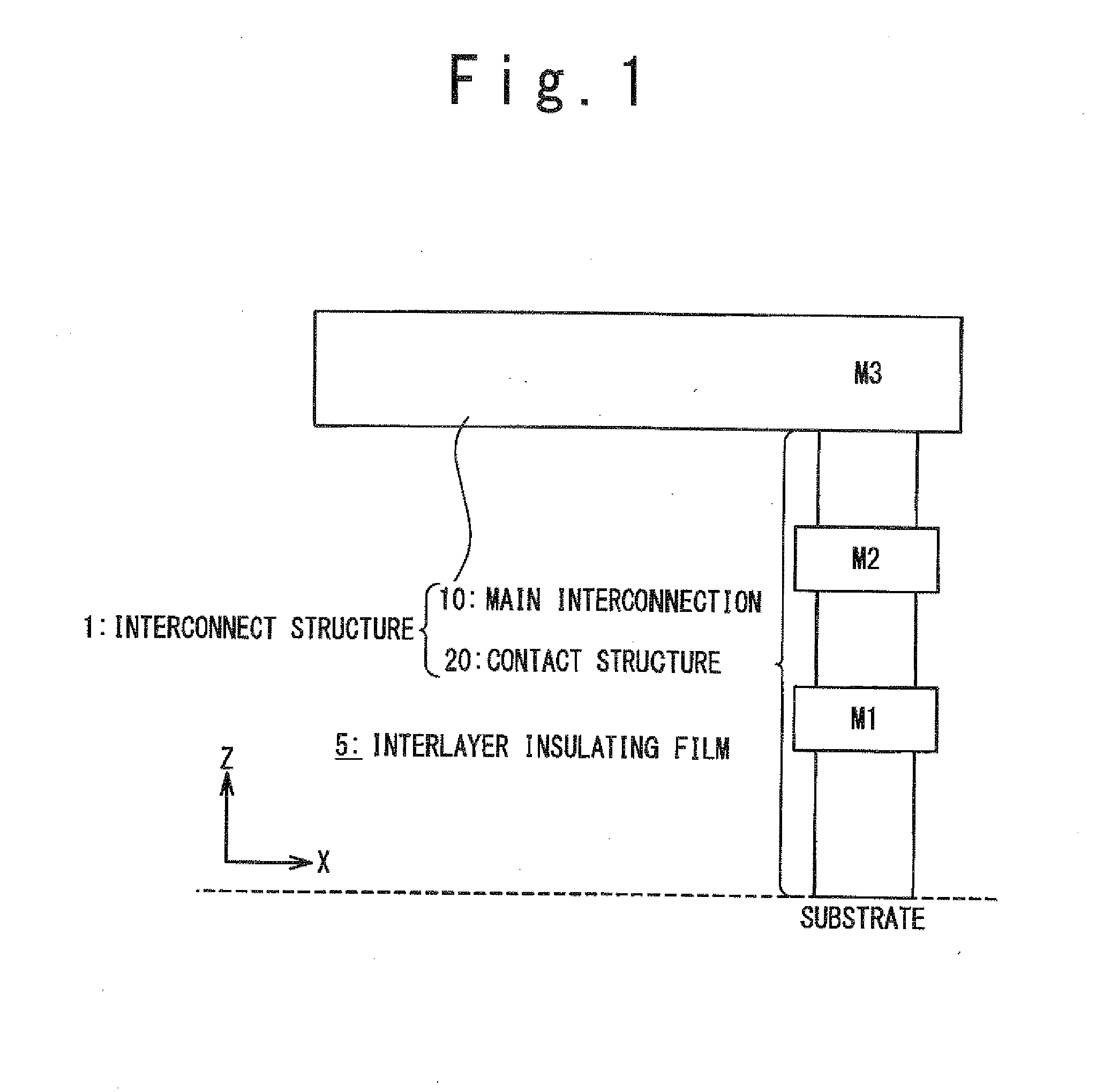
1. Equipotential Interconnect Structure Including Contact Structure

[0040]FIG. 1 schematically shows an interconnect structure 1 in a semiconductor device, which is considered in the present embodiment. In FIG. 1, a plane parallel to a surface of a semiconductor substrate is represented by a XY plane and a direction perpendicular to the XY plane is represented by a Z-direction.

[0041]As shown in FIG. 1, the interconnect structure 1 includes a main interconnection 10 and a contact structure 20 electrically connected to the main interconnection 10. The main interconnection10 is formed in an interconnection layer located above the semiconductor substrate and is parall...


PUM


Abstract

A sensitivity analysis system has a memory device in which an interconnect structure data indicating an interconnect structure included in a semiconductor device is stored. The interconnect structure has: a main interconnection; and a contact structure electrically connected to the main interconnection and extending toward a semiconductor substrate. Parameters contribute to parasitic capacitance of the interconnect structure, and variation of each parameter from a design value caused by manufacturing variability is represented within a predetermined range. The sensitivity analysis system further has: a parameter setting unit that sets the variation to a plurality of conditions within the predetermined range; a capacitance calculation unit that calculates the parasitic capacitance of the interconnect structure in each of the plurality of conditions; and a sensitivity analysis unit that analyzes, based on the calculated parasitic capacitance, response of the parasitic capacitance to variation of the each parameter.

Description

INCORPORATION BY REFERENCE[0001]This application is based upon and claims the benefit of priority from Japanese patent application No. 2009-006504, filed on Jan. 15, 2009, the disclosure of which is incorporated herein in its entirety by reference.BACKGROUND OF THE INVENTION[0002]1. Field of the Invention[0003]The present invention relates to a design technique for a semiconductor device. In particular, the present invention relates to a design technique for a semiconductor device having a contact structure.[0004]2. Description of Related Art[0005]In a manufacturing process of a semiconductor device, an interconnect structure may not be manufactured as expected. That is, physical parameters such as a width and a thickness of an interconnection, a thickness of an interlayer insulating film and the like may vary from their desired design values. Such manufacturing variability affects delay in a circuit. Thus, even if a designed circuit passes timing verification on a computer, an actu...

Claims


Application Information

Patent Timeline
Patent Type & Authority Applications(United States)
IPC IPC(8): G01R27/26
CPCG06F17/5036H01L23/522G06F2217/12G06F30/367G06F2119/18H01L2924/0002Y02P90/02H01L2924/00
Inventor ASAI, YOSHIHIKO
Why Eureka
Try Eureka