Semiconductor integrated circuit and method for designing same

a technology of integrated circuits and semiconductors, applied in the direction of generating/distributing signals, total factory control, instruments, etc., can solve the problem of tens of more time than expected, and achieve the effect of accurate setting of design margins, reducing circuit size, and high accuracy

Inactive Publication Date: 2006-11-09
PANASONIC CORP
View PDF7 Cites 2 Cited by
  • Summary
  • Abstract
  • Description
  • Claims
  • Application Information

AI Technical Summary

Benefits of technology

[0017] According to the first aspect, it is possible to provide a semiconductor integrated circuit in which timing error is not likely to occur even if there is manufacturing variability. The effect of the first aspect is apparent particularly when the logic cells included in the clock circuits are formed by transistors each having a uniform rectangular-shaped diffusion region.
[0019] According to the third aspect, it is possible to more accurately set the design margin as compared to a conventional method. Therefore, it is possible to reduce a circuit size to less than a conventionally required circuit size, while taking account of variations of delay time of clock signals due to deterioration over time of transistors.
[0020] According to the fourth aspect, by obtaining the number of toggles of a clock signal to be supplied to each circuit block, it is made possible to obtain the probability of a change of the clock signal under the real operating environment in a short time period with high accuracy as compared to logical simulation or the like. Therefore, it is possible to redesign a semiconductor integrated circuit, in which timing error is not likely to occur, with more accurate consideration of the clock signal's delay time variation due to deterioration over time of transistors.
[0021] According to the fifth aspect, even after the semiconductor integrated circuit is incorporated into a system, by adjusting the number of toggles of each clock signal, it is made possible to prevent clock signals, which vary with frequencies different from each other, from being supplied. Once such clock signals are supplied, degrees of deterioration over time may become different between transistors, such that a timing error occurs, resulting in a shorter service life of the semiconductor integrated circuit.
[0022] According to the sixth aspect, it is possible to readily verify that logic cells present on a clock path have a specific characteristic (e.g., they are resistant to process variation). Further, by designating a type of logic cell, which should be present on the clock path, for each corresponding type of clock cell, which should not be, but is, present on the clock path, and replacing a logic cell of the designated type with a logic cell which should not be present on the clock path, it is made possible to change a clock circuit such that only the logic cells having a specific characteristic are present on the clock path.
[0023] According to the seventh aspect, even if there is a difference in the number of stages of logic cells between clock paths, it is possible to accurately set a design margin in accordance with a difference in structure between the clock paths, whereby it is possible to reduce a circuit size to less than a conventionally required circuit size.

Problems solved by technology

Further, the progress in finer fabrication technology has increased the integration scale of the clock circuit, and therefore it tends to take more time than before to perform the clock tree analysis or change the design of the clock circuit.
However, the clock signal is one of the most frequently changing signals, and therefore it is required to design the semiconductor integrated circuit after having correctly evaluated delay time variation of the clock signal due to deterioration over time.

Method used


Image

  • Semiconductor integrated circuit and method for designing same
  • Semiconductor integrated circuit and method for designing same
  • Semiconductor integrated circuit and method for designing same

Examples


first embodiment

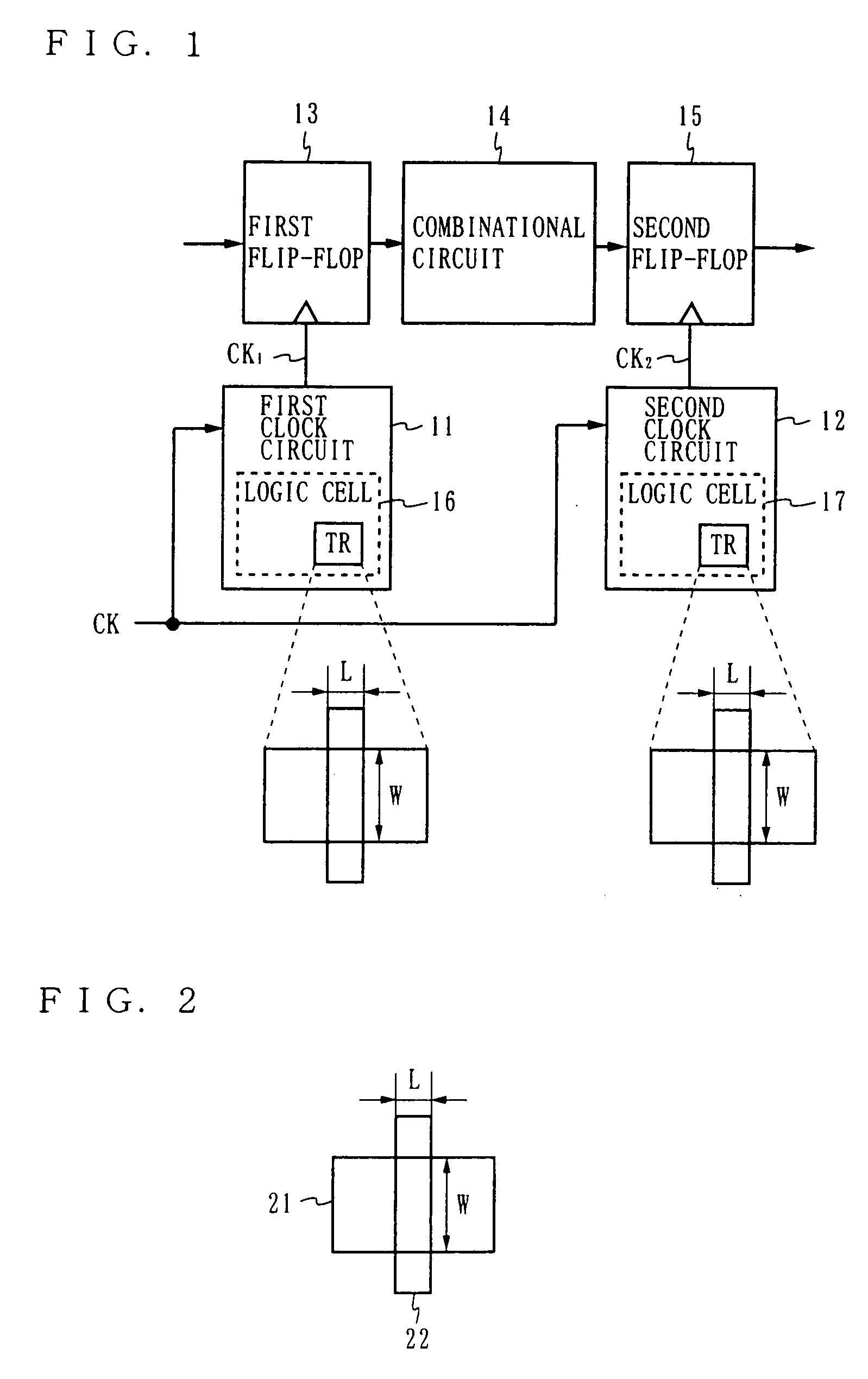
[0049] A first embodiment of the present invention is described with respect to a semiconductor integrated circuit in which logic cells included in clock circuits are formed by transistors of a unified size. FIG. 1 is a diagram showing the structure of the semiconductor integrated circuit according to the present embodiment. The semiconductor integrated circuit shown in FIG. 1 includes a first clock circuit 11, a second clock circuit 12, a first flip-flop 13, a combinational circuit 14, and a second flip-flop 15. Each of the first and second flip-flops 13 and 15 operates in synchronization with a clock signal CK supplied thereto. Specifically, the first clock circuit 11 generates a first clock signal CK1 based on the clock signal CK, and the first flip-flop 13 operates in synchronization with the first clock signal CK1. The second clock circuit 12 and the second flip-flop 15 operate similar to the first clock circuit 11 and the first flip-flop 13, respectively. The combinational cir...

second embodiment

[0062] A second embodiment of the present invention is described with respect to a design method which uses a circuit block, which is designed to operate under a prescribed operating condition, to design a semiconductor integrated circuit so as to operate under an operating condition different from that of the circuit block. Described first is a design method which uses a circuit block, which is designed to operate at a prescribed threshold voltage, to design a semiconductor integrated circuit so as to operate at a threshold voltage different from that of the circuit block (see FIG. 6). A semiconductor integrated circuit 30 shown in FIG. 6 includes an upstream clock circuit 31, a circuit block 32, a second downstream clock circuit 35, and a second flip-flop 36. The semiconductor integrated circuit 30 is designed to operate at a prescribed threshold voltage (hereinafter, referred to as a “second threshold voltage VT2”). The circuit block 32 includes a first downstream clock circuit 3...

third embodiment

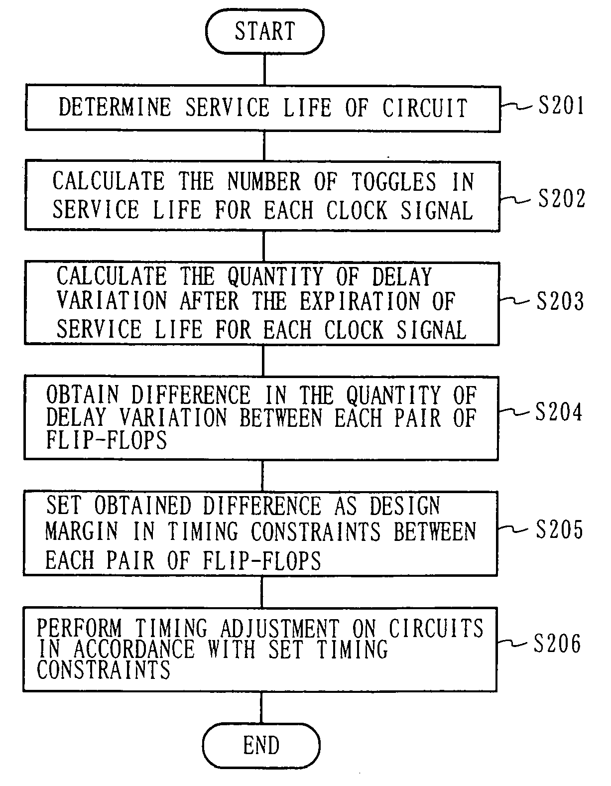
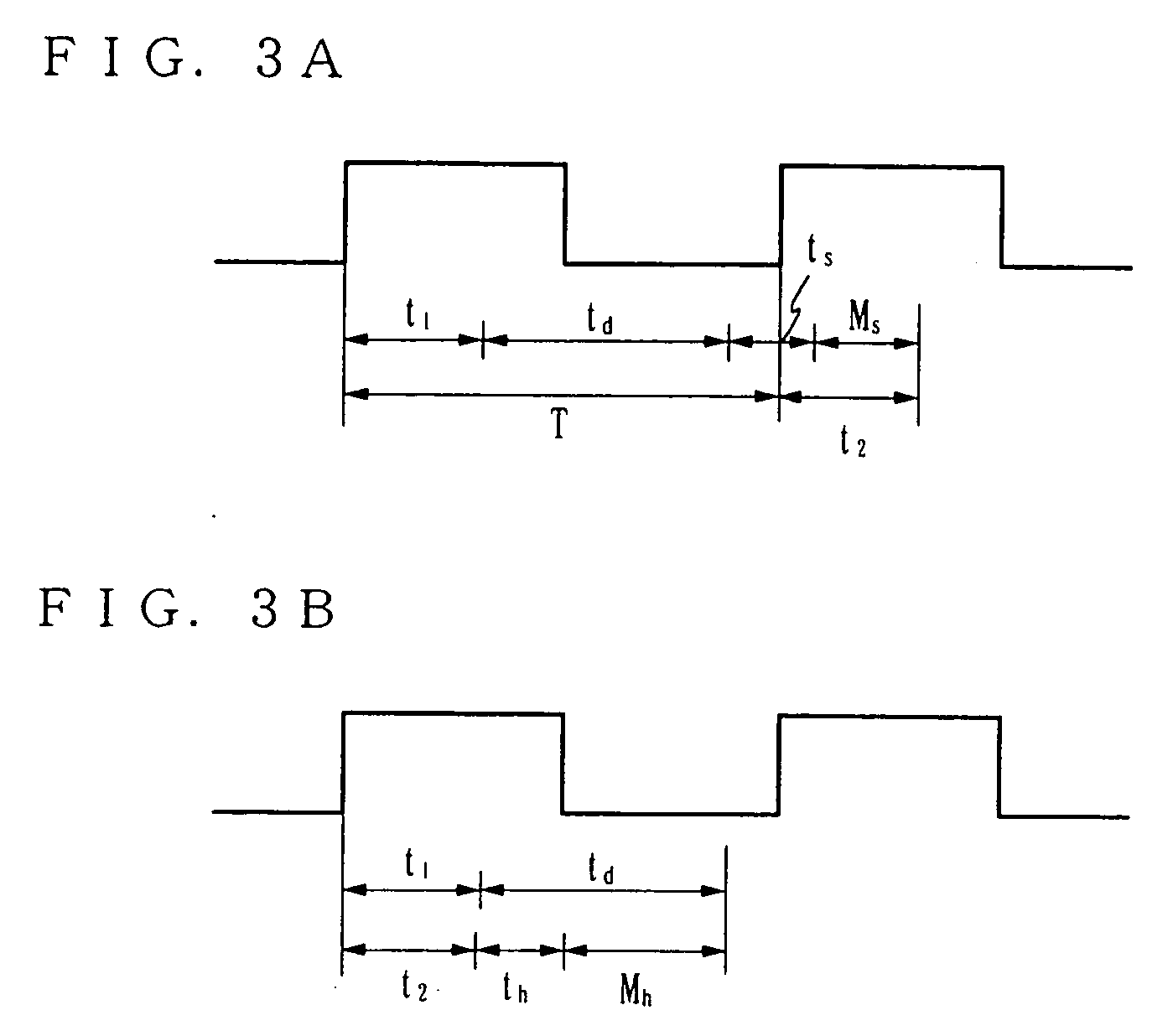
[0070] A third embodiment of the present invention is described with respect to a method for designing a semiconductor integrated circuit which takes account of variations in delay time of clock signals due to deterioration over time of transistors. In general, a transistor deteriorates depending on the length of time periods for which a prescribed signal voltage is applied thereto. Accordingly, a delay time of a circuit formed by transistors is increased with the passage of time. In most cases, the length of a time period for which a clock signal is at a high level is the same as the length of a time period for which the signal is at a low level. Accordingly, by counting the number of times when the clock signal is changed to a prescribed value (hereinafter, referred to as the “number of toggles”), it is possible to calculate the length of time periods for which the clock signal is at the prescribed value, whereby it is possible to previously estimate how much deterioration occurs ...


PUM


Abstract

The present invention provides a semiconductor integrated circuit in which timing error is not likely to occur even if there is manufacturing variability. Logic cells 16 and 17, which are included in first and second clock circuits 11 and 12, respectively, are formed by transistors of a unified size. Even if there is manufacturing variability, delay time t1 of the first clock circuit 11 and delay time t2 of the second clock circuit 12 are increased or decreased by the same amount of time. Because of this, timing error is not likely to occur in a second flip-flop 15. A logic cell included in each clock cell may be formed by a transistor having a uniform rectangular-shaped diffusion region.

Description

BACKGROUND OF THE INVENTION [0001] 1. Field of the Invention [0002] The present invention relates to a semiconductor integrated circuit, which operates in synchronization with a clock signal, and a method for designing such a semiconductor integrated circuit. [0003] 2. Description of the Background Art [0004] In most cases, a semiconductor integrated circuit including a logic circuit operates in synchronization with an externally supplied clock signal or a clock signal which is internally generated based on an externally supplied signal. In general, the semiconductor integrated circuit includes a plurality of flip-flops and a circuit which generates a clock signal to be supplied to each flip-flop based on a supplied clock signal (hereinafter, such a circuit is referred to as a “clock circuit”). In order to allow the semiconductor integrated circuit to operate accurately, it is necessary to supply an appropriate clock signal to each flip-flop. Further, in order to reduce power consum...

Claims


Application Information

Patent Timeline
Patent Type & Authority Applications(United States)
IPC IPC(8): G06F17/50G06F1/10G06F9/45H01L21/82H03L7/06
CPCG06F1/10G06F17/5031G06F2217/12G06F17/5059G06F17/5045G06F30/35G06F2119/18G06F30/3312G06F30/30Y02P90/02
Inventor MATSUMURA, YOICHIOHASHI, TAKAKOFUJIMURA, KATSUYAITOH, CHIHIROTANIGUCHI, HIROKI
Owner PANASONIC CORP
Why Eureka
Try Eureka