Die rearrangement package structure and method thereof

a package and rearrangement technology, applied in the direction of semiconductor devices, semiconductor/solid-state device details, electrical apparatus, etc., can solve the problems of reduced reliability of the package, solder ball is not easy to be damaged, and the conventional lead frame package technology is not good enough for high-density pins, etc., to achieve accurate positioning at the desired position

Inactive Publication Date: 2009-12-10
CHIPMOS TECH INC
View PDF23 Cites 23 Cited by
  • Summary
  • Abstract
  • Description
  • Claims
  • Application Information

AI Technical Summary

Benefits of technology

[0009]According the problems described in prior art, the main object of the present invention is to provide a carrier board with a package structure formed thereon. Because of the package structure, the dice are able to relocate on another carrier board, and each of the dice is able to accurately locate at the desired position.

Problems solved by technology

Therefore, the conventional lead frame package technology is not good enough for high density pins, and a Ball Grid Array (BGA) package technology is developed.
The BGA package technology is able to package the dice with high density pins and the solder ball is not easy to be damaged.
However, when the number of the pads on the active surface of the dice is increased and the interval between the pads is too small, the signal in the dice will be overlapped or interrupted and the reliability of the package is decrease because of the small interval of the dice.
Therefore, when the die is become smaller and smaller, the package technologies described above are not able to satisfy.
Because the die is very thin, the package structure is also very thin.
When the package structure is moved from the substrate, the stress from the package structure itself will let the package structure bend over and the difficulty of the sawing process is increased.
Therefore, the dice are not able to locate correctly and the solder ball process is not able to locate at the right position and the reliability of the package structure is decreased.

Method used


Image

  • Die rearrangement package structure and method thereof
  • Die rearrangement package structure and method thereof
  • Die rearrangement package structure and method thereof

Examples


Embodiment Construction

[0034]The detailed description of the present invention will be discussed in the following embodiments, which are not intended to limit the scope of the present invention, but can be adapted for other applications. While drawings are illustrated in details, it is appreciated that the quantity of the disclosed components may be greater or less than that disclosed, except expressly restricting the amount of the components.

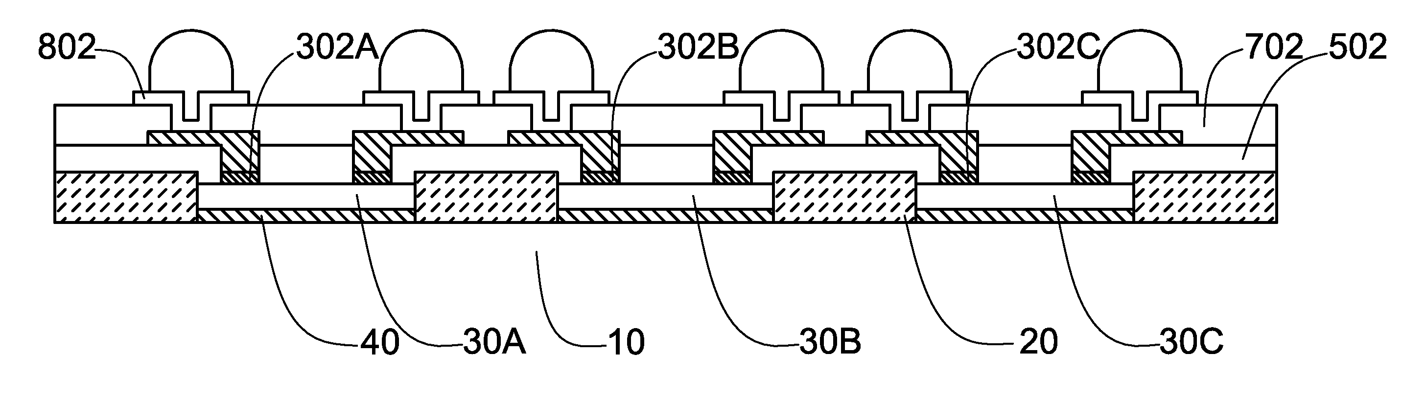
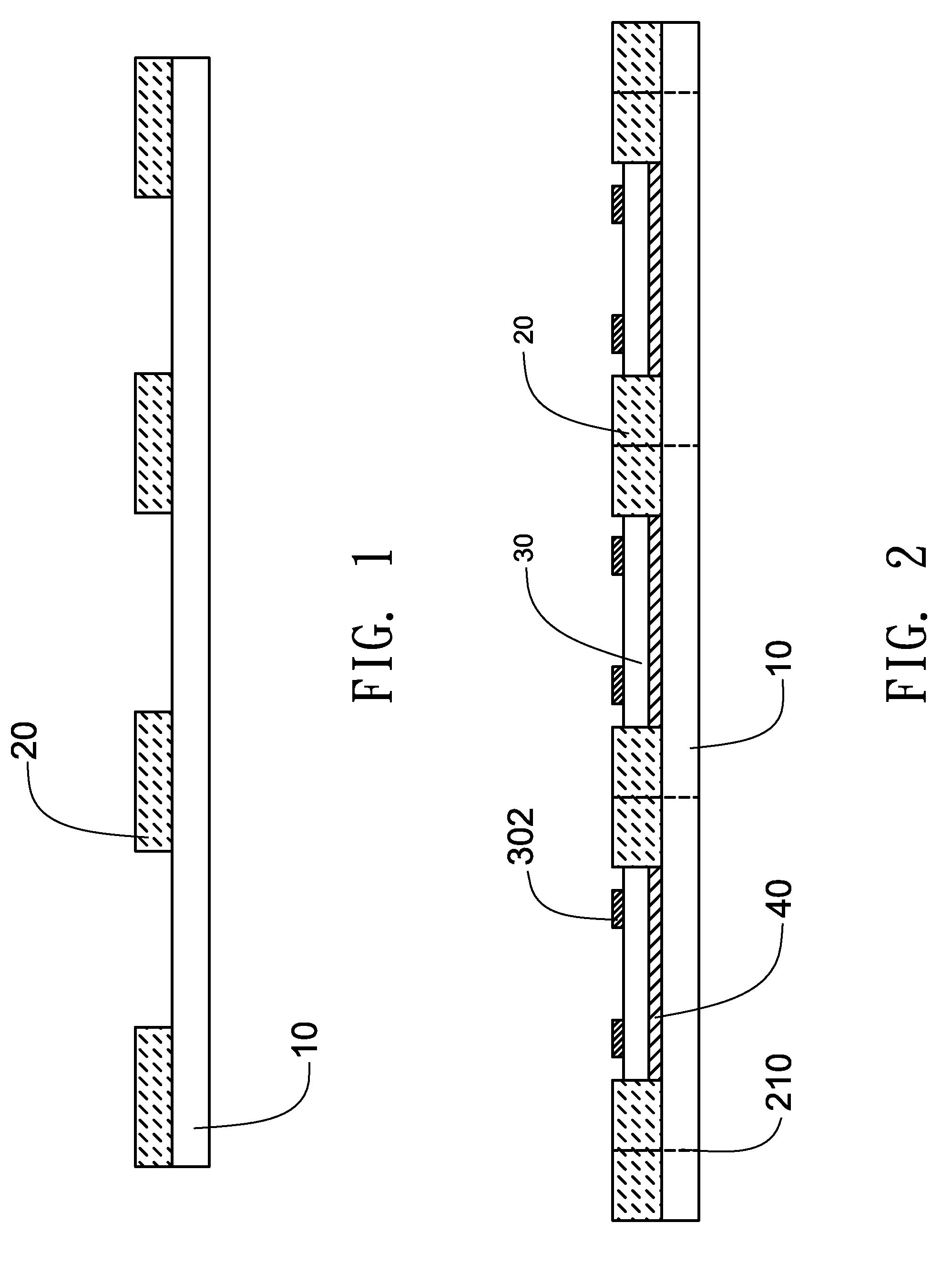
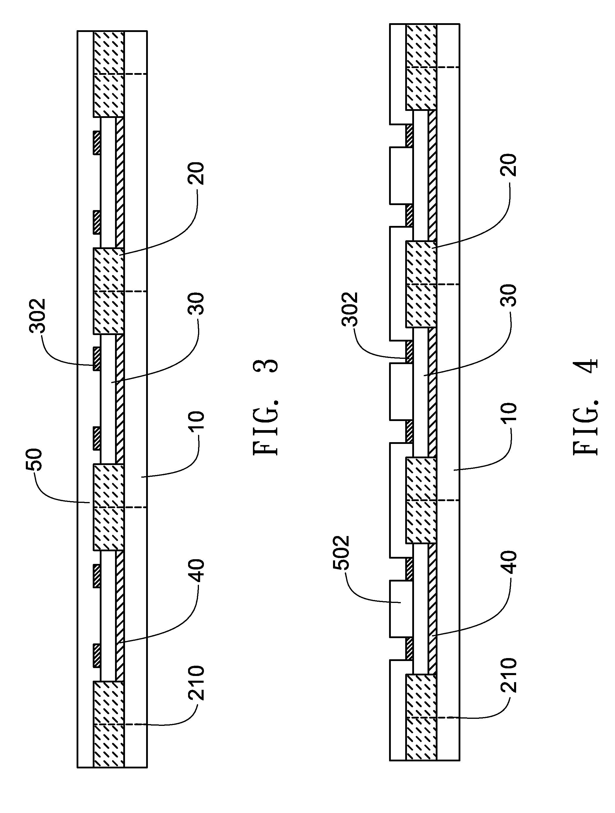
[0035]In the present semiconductor package method, the wafer done with the front end process will do a thinning process, such as thinning the wafer to be 2˜20 mil thick. Then, a sawing process is performed to saw the wafer to be a plurality of dies and a pick and place apparatus is used to relocate the die in another substrate. Obviously, the dice in the new carrier board able to have an interval larger than the die. Therefore, those die are able to have wider intervals and the pads on the dice are able to reorganize well.

[0036]First of all, a wafer (not shown) is pr...


PUM


Abstract

A die rearrangement package structure is provided and includes a die; an encapsulated structure is covered around the four sides of the die to expose the active surface and the reverse side of the die; a patterned protective layer is formed on the encapsulated structure and the active surface of the die, and the pads is to be exposed; one end of fan-out patterned metal layer is electrically connected the pads and other end is extended to cover the patterned protective layer; patterned second protective layer is provided to cover the patterned metal layer to expose the portions surface of the patterned metal layer; patterned UBM layer is formed on the exposed surface of the patterned metal layer; and a conductive component is formed on the patterned UBM layer, and electrically connected the patterned metal layer.

Description

BACKGROUND OF THE INVENTION[0001]1. Field of the Invention[0002]The present invention is related to a package structure and method thereof, and more particularly, is related to a die rearrangement package structure and method thereof by using a RDL.[0003]2. Description of the Prior Art[0004]The technology development in semiconductor is very fast, the microlize semiconductor dice is needed to have more functions therein. Thus, the microlize semiconductor dice needs to have more I / O pads within very tiny area, and the density of the pins is increased. Therefore, the conventional lead frame package technology is not good enough for high density pins, and a Ball Grid Array (BGA) package technology is developed. The BGA package technology is able to package the dice with high density pins and the solder ball is not easy to be damaged.[0005]Because the 3C products, such as cell phone, portable digital assistant (PDA), or IPOD, are become more and more popular, the system die has to insta...

Claims


Application Information

Patent Timeline
Patent Type & Authority Applications(United States)
IPC IPC(8): H01L21/50H01L21/768H01L23/498
CPCH01L21/568H01L24/83H01L23/3128H01L23/5389H01L24/97H01L2221/68345H01L2224/83191H01L2224/97H01L2924/01074H01L2924/01082H01L2924/01094H01L2924/15174H01L2924/15311H01L21/6835H01L2924/014H01L2924/01033H01L2924/01005H01L2224/82H01L2924/181H01L2924/00
Inventor HUANG, CHENG-TANG
Owner CHIPMOS TECH INC
Why Eureka
Try Eureka