Method and system for implementing pattern matching of integrated circuit features using voronoi diagrams

a technology of integrated circuits and features, applied in error detection/correction, program control, instruments, etc., can solve the problems of a large percentage image processing tools provide a simpler user interface, and require special programming skills in order to achieve the effect of reducing the number of false positives and false negatives

Active Publication Date: 2009-12-17
SIEMENS PROD LIFECYCLE MANAGEMENT SOFTWARE INC
View PDF13 Cites 16 Cited by
  • Summary
  • Abstract
  • Description
  • Claims
  • Application Information

AI Technical Summary

Benefits of technology

[0008]The foregoing discussed drawbacks and deficiencies of the prior art are overcome or alleviated, in an exemplary embodiment, by a method for implementing pattern matching of integrated circuit features, including computing Voronoi edge regions for both a reference configuration and a search space of an integrated circuit design to be searched and presenting the computed Voronoi edge regions of the reference configuration to a user; receiving one or more selected bisectors of the Voronoi computed reference configuration from the user, indicative of user identified salient regions of design shapes and / or corners to be searched, so as to define one or more search elements, wherein a search element comprises a given bisector and a pair of Voronoi edge regions bounded thereby; constructing a search pattern from the one or more search elements defined from the reference configuration; examining the search space for matching sequences with respect to the search pattern; and highlighting resulting matching patterns in the search space for the user.
[0009]In another embodiment, a computer program product includes a computer readable computer program code for implementing pattern matching of integrated circuit features; and instructions for causing a computer to implement a method, the method further including computing Voronoi edge regions for both a reference configuration and a search space of an integrated circuit design to be searched and presenting the computed Voronoi edge regions of the reference configuration to a user; receiving one or more selected bisectors of the Voronoi computed reference configuration from the user, indicative of user identified salient regions of design shapes and / or corners to be searched, so as to define one or more search elements, wherein a search element comprises a given bisector and a pair of Voronoi edge regions bounded thereby; constructing a search pattern from the one or more search elements defined from the reference configuration; examining the search space for matching sequences with respect to the search pattern; and highlighting resulting matching patterns in the search space for the user.
[0010]A system for implementing pattern matching of integrated circuit features includes a computing network including a processing device in communication with one or more computer memory storage devices; and the computing network further configured to implement a method, the method including computing Voronoi edge regions for both a reference configuration and a search space of an integrated circuit design to be searched and presenting the computed Voronoi edge regions of the reference configuration to a user; receiving one or more selected bisectors of the Voronoi computed reference configuration from the user, indicative of user identified salient regions of design shapes and / or corners to be searched, so as to define one or more search elements, wherein a search element comprises a given bisector and a pair of Voronoi edge regions bounded thereby; constructing a search pattern from the one or more search elements defined from the reference configuration; examining the search space for matching sequences with respect to the search pattern; and highlighting resulting matching patterns in the search space for the user.

Problems solved by technology

However, such tools also require specialized programming skills in order to encode the reference pattern.
On the other hand, the image processing tools provide a simpler user interface, but suffer from a high percentage of false positives and false negatives because they do not provide for saliency.

Method used


Image

  • Method and system for implementing pattern matching of integrated circuit features using voronoi diagrams
  • Method and system for implementing pattern matching of integrated circuit features using voronoi diagrams
  • Method and system for implementing pattern matching of integrated circuit features using voronoi diagrams

Examples


Embodiment Construction

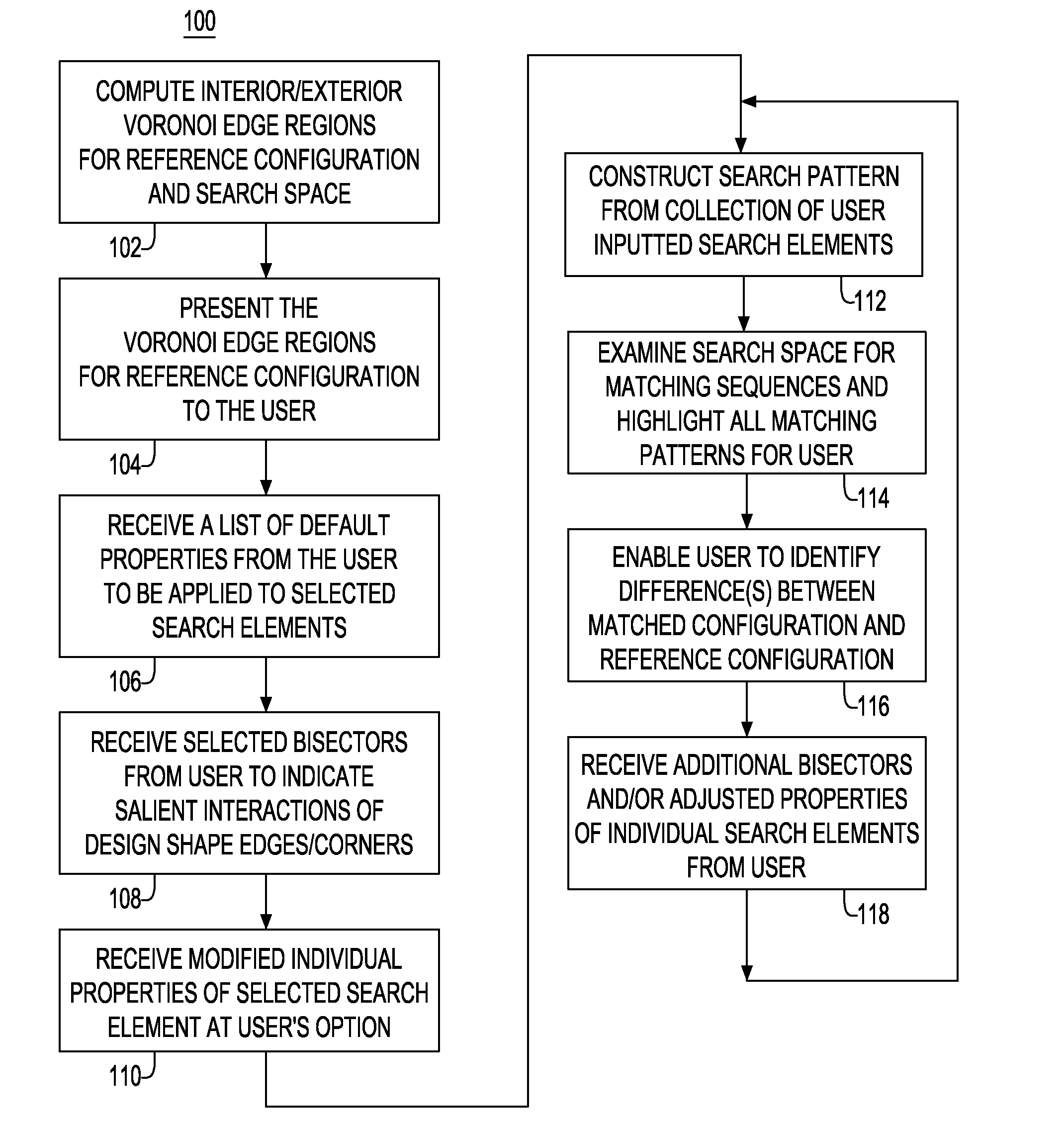
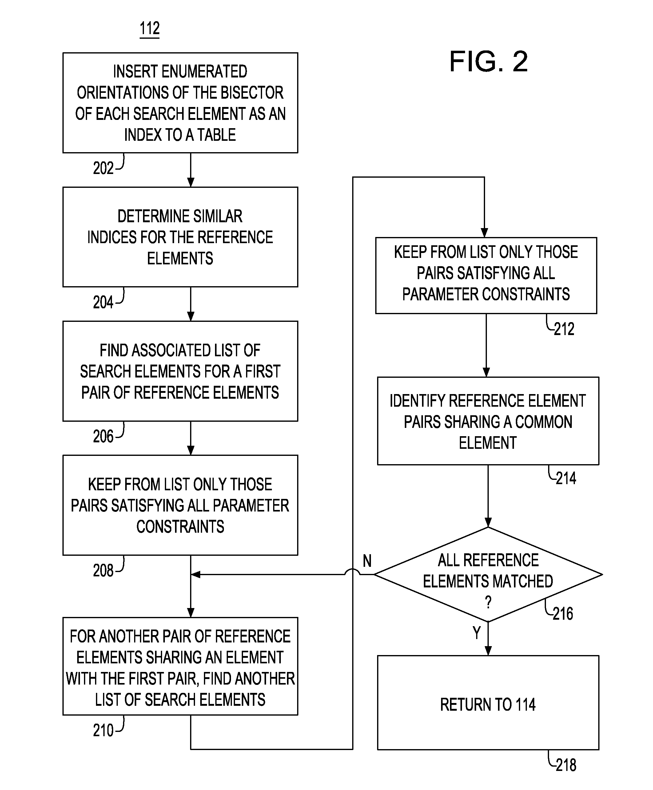
[0019]Disclosed herein is a method and system for implementing pattern matching of integrated circuit features using Voronoi diagrams. Briefly stated, the space between nearest neighbor edges of an integrated circuit design is partitioned into Voronoi regions associated with pairs of interacting edges or corners. The user can either create a new layout design that represents the target pattern of interest or locate one such exemplar in the original design itself to be searched. The user then selects those Voronoi regions that define the salient interactions, optionally selects parametric constraints for the regions, and then the system locates similar patterns elsewhere in the design. If the returned similar patterns turn out not to correspond to the exact set the user intended, the user can subsequently modify the selections, constraints or properties based on a comparison between the target pattern and the unwanted similar pattern. Moreover, the system may also be used in combinat...


PUM


Abstract

A method for implementing pattern matching of integrated circuit features includes computing Voronoi edge regions for both a reference configuration and a search space of an integrated circuit design to be searched and presenting the computed Voronoi edge regions of the reference configuration to a user; receiving one or more selected bisectors of the Voronoi computed reference configuration from the user, indicative of user identified salient regions of design shapes and/or corners to be searched, so as to define one or more search elements, wherein a search element comprises a given bisector and a pair of Voronoi edge regions bounded thereby; constructing a search pattern from the one or more search elements defined from the reference configuration; examining the search space for matching sequences with respect to the search pattern; and highlighting resulting matching patterns in the search space for the user.

Description

BACKGROUND[0001]The present invention relates generally to integrated circuit device design techniques and, more particularly, to a method and system for implementing pattern matching of integrated circuit features using Voronoi diagrams.[0002]In designing an integrated circuit (IC) device, engineers or designers typically rely on computer design tools to help create an IC schematic or design, which can include a multitude of individual devices, such as transistors, coupled together to perform a certain function. To actually fabricate the IC device in or on a semiconductor substrate, the IC device schematic must be translated into a physical representation or layout, which itself can then be transferred onto a semiconductor substrate. Computer aided design (CAD) tools can be used to assist layout designers with translating the discrete circuit elements into shapes, which will embody the devices themselves in the completed IC device. These shapes make up the individual components of ...

Claims


Application Information

Patent Timeline
Patent Type & Authority Applications(United States)
IPC IPC(8): G06K9/62
CPCG06K9/00476G06K9/6263G06K9/626G06K9/6253G06V30/422G06F18/40G06F18/24765G06F18/2178
Inventor MONKOWSKI, MICHAEL D.
Owner SIEMENS PROD LIFECYCLE MANAGEMENT SOFTWARE INC
Why Eureka
Try Eureka