Conductive Contact Holder

a technology of contact holder and conductive material, which is applied in the direction of connection contact member material, printed circuit, instruments, etc., can solve the problems of durability and assembly difficulties, and achieve the effect of high integration and simple and easy assembly structur

Active Publication Date: 2009-12-17
NHK SPRING CO LTD
View PDF26 Cites 13 Cited by
  • Summary
  • Abstract
  • Description
  • Claims
  • Application Information

AI Technical Summary

Benefits of technology

[0016]According to the present invention, there is provided a conductive contact holder including: an insulating holder member that is made of an insulating material, and includes a first insertion hole through which a signal conductive contact inputting and outputting a signal to and from a circuit is inserted over substantially its full length; and a conductive block member that is made of a conductive material, and includes a second insulation hole through which the ground conductive contact is inserted in partial contact therewith. With this, the conductive contact holder having a simple and easily assembled structure can deal with a high-frequency signal and with high integration and miniaturization of a test object.

Problems solved by technology

This arrangement, however, causes a problem of its durability and difficulties in assembly.

Method used


Image

  • Conductive Contact Holder
  • Conductive Contact Holder
  • Conductive Contact Holder

Examples


Embodiment Construction

[0051]Best modes (hereinafter, “embodiments”) for carrying out the invention will be described with reference to the accompanying drawings. Note that the drawings are schematic and the relationship between the thickness and the width of elements, the ratio of the thicknesses of the elements, and the like may be different from those actually measured. Needless to say, some elements may be different in the dimensional relationship or ratio in the drawings.

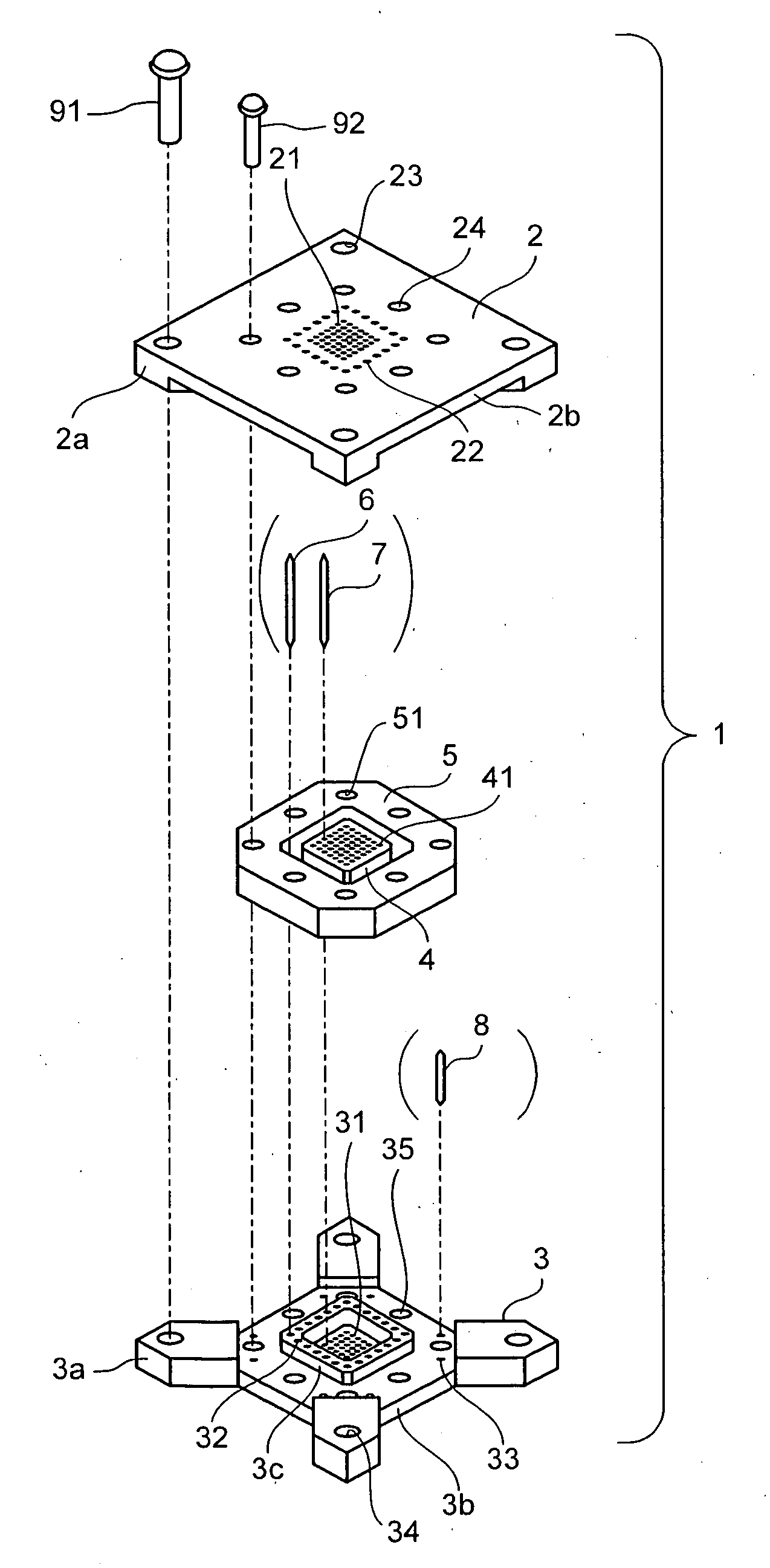
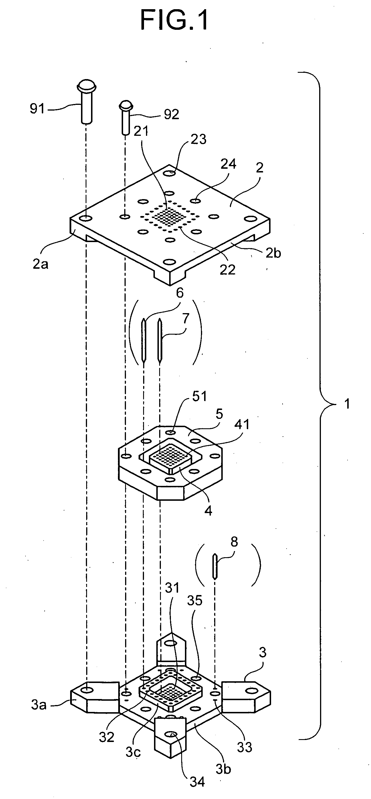
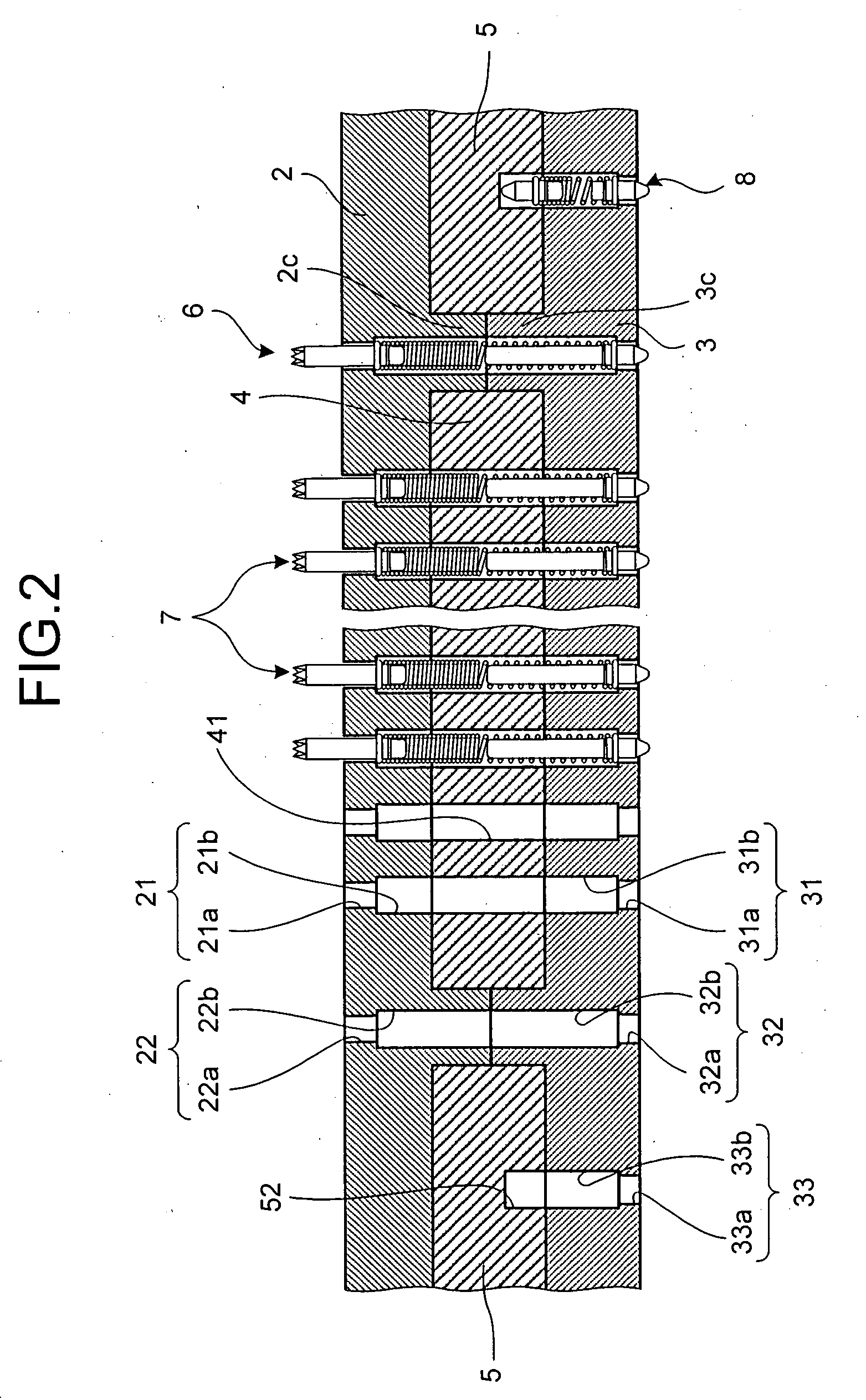
[0052]FIG. 1 is an exploded perspective view of a structure of a conductive contact holder according to an embodiment of the present invention. FIG. 2 is a vertical cross-sectional view of relevant portions of the conductive contact holder according to the present embodiment. FIG. 3 is a partial enlarged view of FIG. 2. A conductive contact holder 1 shown in FIGS. 1 to 3 constitutes at least part of a conductive contact unit that tests electrical characteristics of a predetermined circuit typified by a semiconductor integrated circui...


PUM


Abstract

A conductive contact holder includes an insulating holder member and a conductive block member. The insulating holder member is made of an insulating material and includes a first insertion hole through which a signal conductive contact inputting and outputting a signal to and from a circuit is directly inserted over substantially its full length. The conductive block member His made of a conductive material and includes a second insertion hole through which the ground conductive contact is inserted in partial contact therewith.

Description

TECHNICAL FIELD[0001]The present invention relates to a conductive conduct holder that holds conductive contacts used for current testing of a circuit such as a semiconductor integrated circuit.BACKGROUND ART[0002]Upon current testing of a semiconductor integrated circuit such as an integrated circuit (IC) chip, a conductive contact unit has been used that has a plurality of conductive contacts at predetermined positions corresponding to an arrangement pattern of external connecting electrodes provided in the semiconductor integrated circuit. Such a conductive contact unit includes a conductive contact holder formed of an insulating material for holding the conductive contacts.[0003]To realize high-speed computing, semiconductor integrated circuits in recent years have been configured to operate by an electrical signal (a high frequency signal) having a high frequency of about several hundred megahertz (MHz) to several hundred gigahertz (GHz). Further, semiconductor integrated circu...

Claims


Application Information

Patent Timeline
Patent Type & Authority Applications(United States)
IPC IPC(8): H01R4/58
CPCG01R1/0466G01R1/07371G01R1/06772G01R1/0483G01R1/073
Inventor NAKAYAMA, HIROSHIHIRONAKA, KOHEIMABUNE, YOSUKE
Owner NHK SPRING CO LTD
Why Eureka
Try Eureka