Liquid crystal panel and liquid crystal display device

Active Publication Date: 2009-12-24
MERCK PATENT GMBH
View PDF16 Cites 9 Cited by
  • Summary
  • Abstract
  • Description
  • Claims
  • Application Information

AI Technical Summary

Benefits of technology

[0017]The present invention is attained in view of the above problems. An object of the present invention is to provide a practical liquid crystal panel and a practical

Problems solved by technology

However, a liquid crystal display device employing the TN mode has disadvantages such as a slow response and a narrow viewing angle.
However, the MVA mode liquid crystal display has disadvantages such that (i) a production process is complex and (ii) as with the TN mode liquid crystal display device, a response speed is slow.
However, the IPS mode also has a disadvantage such that a response speed is slow as with the TN mode and the MVA mode.
Further, the IPS mode is not suitable for mobile devices or in-vehicle devices for which a high speed at a low temperature is required.
Therefore, a factor to increase cost is inherent in the OCB mode.
Further, the OCB mode is inferior in a vi

Method used


Image

  • Liquid crystal panel and liquid crystal display device
  • Liquid crystal panel and liquid crystal display device
  • Liquid crystal panel and liquid crystal display device

Examples


embodiment 1

[0051]One embodiment of the present invention is explained below with reference to FIGS. 1 to 17(b).

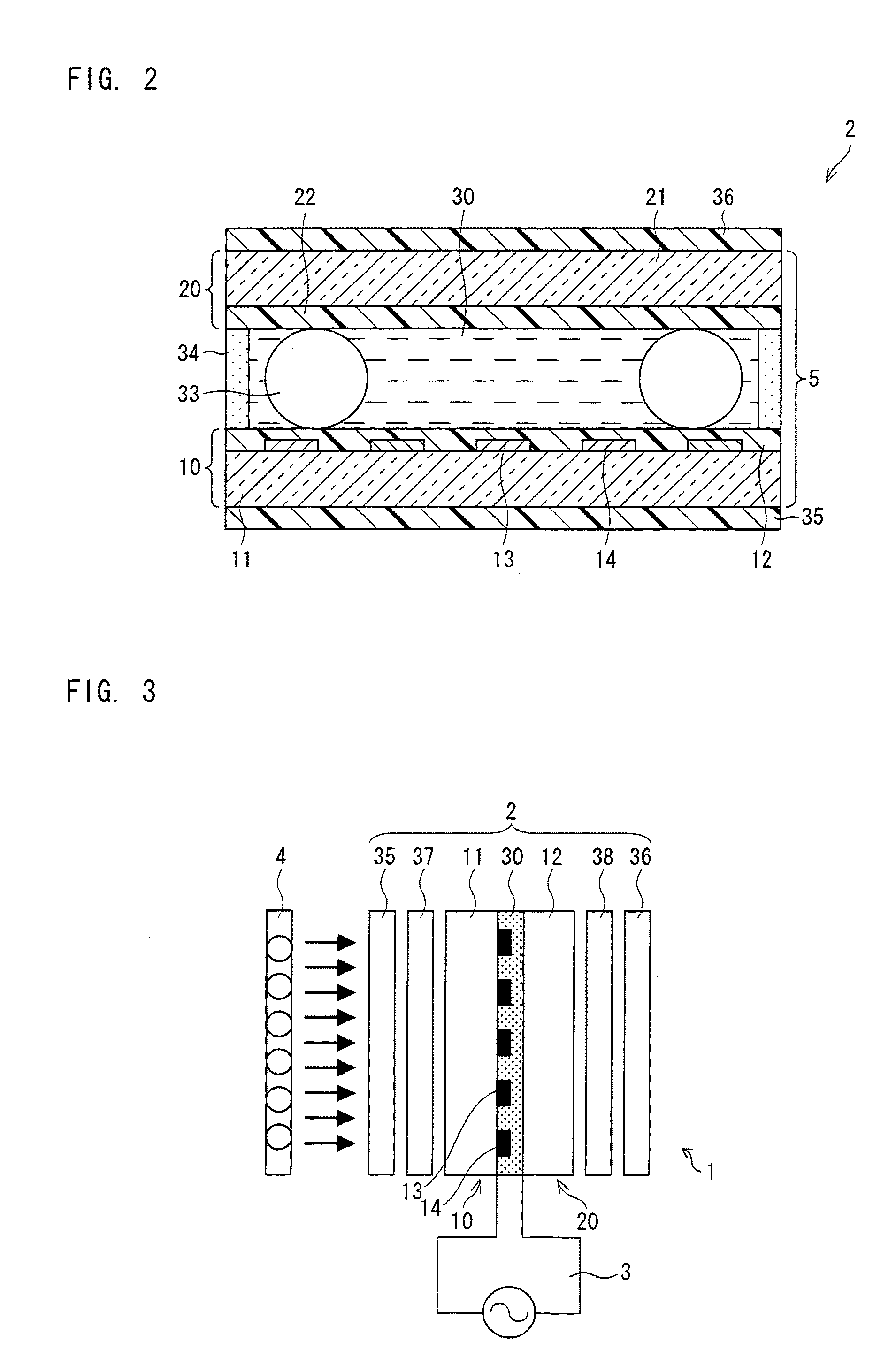
[0052]FIG. 3 is an exploded cross sectional view schematically illustrating an outline configuration of a liquid crystal display device according to the present embodiment.

[0053]As illustrated in FIG. 3, a liquid crystal display device 1 of the present embodiment includes a liquid crystal panel 2, a driving circuit 3, and a backlight 4 (illumination device). Configurations of the driving circuit 3 and the backlight 4 are the same as configurations of conventional driving circuit and backlight, and explanations thereof are omitted.

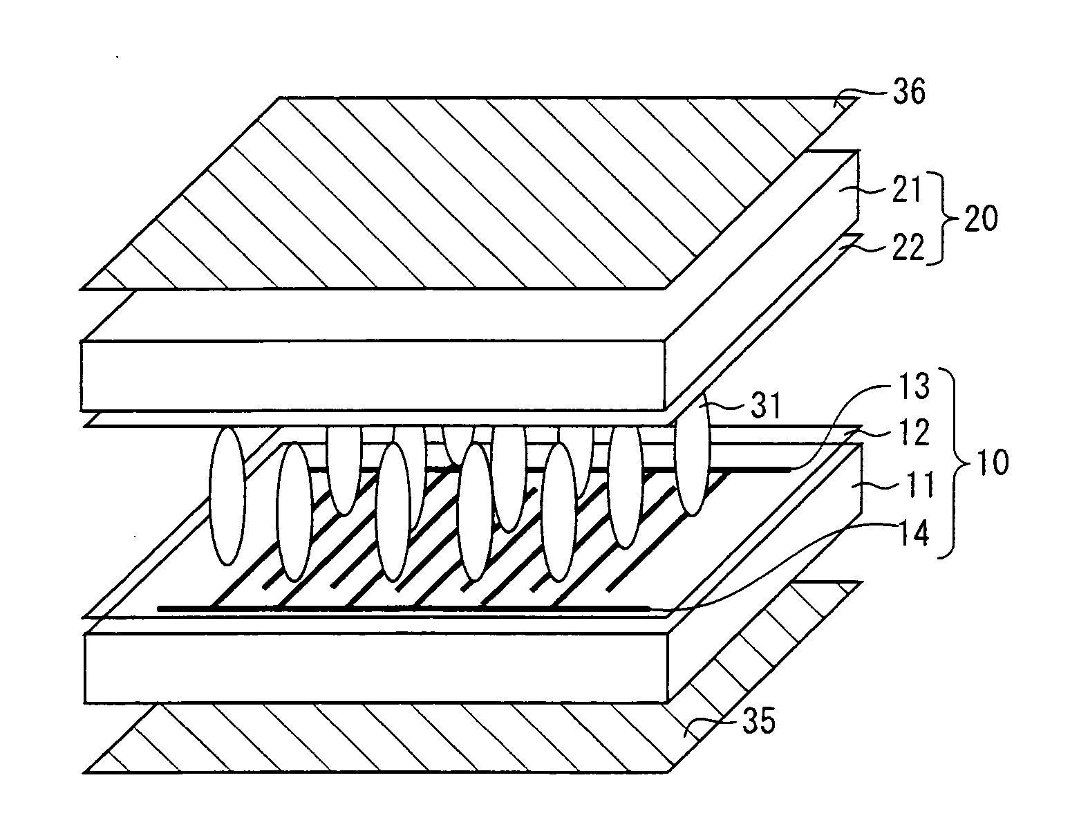
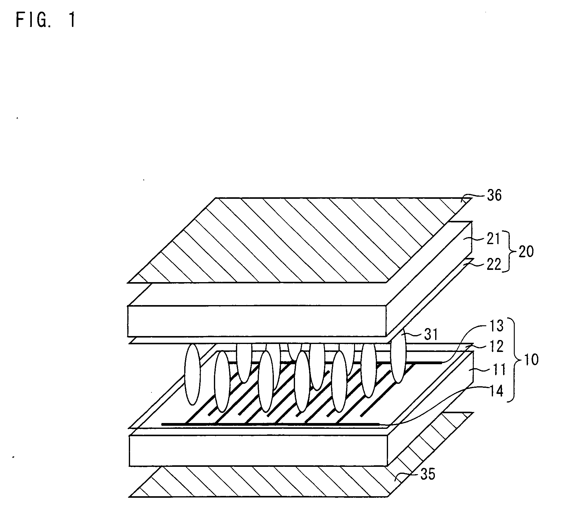
[0054]FIGS. 1 and 2 show a typical panel configuration as one example of the liquid crystal panel 2 according to the present embodiment.

[0055]FIG. 1 is an exploded perspective view schematically illustrating an outline configuration of a substantial part of the liquid crystal panel 2. FIG. 2 is a cross sectional view schematically illustrating an outline conf...

example 1

[0094]First, an alignment film material “JALS-204” (Product Name, 5% by weight (solid content), γ-butyrolactone solution, produced by JSR Corporation) was applied, by a spin coat method, on a glass substrate that was provided with comb-teeth electrodes 13 and which were made of ITO and that had an electrode width L of 4 μm, an electrode spacing S of 4 μm, and an electrode thickness of 1000 A. Then, the glass substrate with the alignment film material was baked at 200° C. for 2 hours so as to form a substrate 10. A thickness of an alignment film 12 obtained was 600 Å (60 nm).

[0095]Next, an alignment film 22 that was identical to the alignment film 12 was formed on a glass substrate 22 so as to form a substrate 20 in the same manner as the substrate 10 except that the comb-teeth shape electrodes and 14 were not provided on the glass substrate 21.

[0096]Subsequently, on the substrate 10, resin beads “Micropearl SP” (Product Name, manufactured by Sekisui Chemical Co. Ltd.), as a spacer 3...

example 2

[0113]Forty liquid crystal panels 2 each having the configuration as shown in FIG. 2 were fabricated in the same manner as Example 1 except that “MLC-6269-000” (Product Name, manufactured by Merck Ltd., p-type nematic liquid crystal material, Δε=17.7 and Δn=0.0984) was used as the liquid crystal material and the electrode width L, the electrode spacing S, and the cell gap d were variously changed.

[0114]Next, at 25° C., while an applied voltage was varied from 0V to 20V, a voltage-transmittance characteristic of each of the liquid crystal panels 2 was measured. In the measurement, a rectangular wave of 30 Hz was applied and a wavelength of light for measurement was 550 nm. A relation of the electric application direction and the transmission axis directions of the polarizers 35 and 36 at that time was as shown in FIG. 4. Table 1 shows all relations of the electrode width L, the electrode spacing S, and the maximum transmittance Tmax of the liquid crystal panels 2 each having the cell...


PUM


Abstract

A liquid crystal panel includes: a p-type liquid crystal material sandwiched by a pair of substrates and comb-teeth shape electrodes for applying, to the p-type liquid crystal material, an electric field parallel to a substrate surface. The p-type liquid crystal material is aligned vertically with respect to the substrate surface at the time when no electric field is applied. The comb-teeth shape electrodes have an electrode width of 5 μm or less, and an electrode spacing of 15 μm or less. A product of a dielectric constant anisotropy Δε and a refractive index anisotropy Δn of the p-type liquid crystal material is 1.3 or more and 3.1 or less.

Description

[0001]This Nonprovisional application claims priority under 35 U.S.C. § 119(a) on Patent Application No. 2008-159390 filed in Japan on Jun. 18, 2008, International Application No. PCT / JP2009 / 052835 filed on Feb. 19, 2009, and Patent Application No. 2009-131560 filed in Japan on May 29, 2009, and the entire contents of which are hereby incorporated by reference.FIELD OF THE INVENTION[0002]The present invention relates to a liquid crystal panel and a liquid crystal display device, in particular, to a liquid crystal panel and a liquid crystal display device each controlling transmission of light by causing bend distortion of a liquid crystal layer by voltage application.BACKGROUND OF THE INVENTION[0003]Liquid crystal display devices have a small thickness, a light weight, and a low power consumption as characteristics, and are used in various fields. Display performance of such liquid crystal display devices is drastically improved year by year. As a result, recently the display perfor...

Claims


Application Information

Patent Timeline
IPC IPC(8): C09K19/02G02F1/1343G02F1/1337
CPCC09K19/3003C09K19/3028C09K19/3059C09K19/3068C09K19/322G02F2001/13712C09K2019/3019C09K2019/3021G02F1/134363G02F2001/133397G02F2001/133742C09K2019/301G02F1/133397G02F1/133742G02F1/13712
Inventor ISHIHARA, SHOICHISAKURAI, TAKEHISAKOZAKI, SHUICHI
Owner MERCK PATENT GMBH
Why Eureka
Try Eureka