Electronic device substrate, electronic device and methods for making same

a technology of electronic devices and substrates, applied in the direction of conductive pattern formation, other domestic objects, electrical apparatus construction details, etc., can solve the problems of poor adhesiveness of functional plating 123, deterioration of adhesiveness with sealing resin, and lowering the reliability of electronic devices, so as to prevent a crack in the production process and reduce the mounting area

Inactive Publication Date: 2009-12-31
RENESAS ELECTRONICS CORP
View PDF4 Cites 7 Cited by
  • Summary
  • Abstract
  • Description
  • Claims
  • Application Information

AI Technical Summary

Problems solved by technology

However, the conventional electronic devices each have the following problems.
The composition as shown in FIG. 11 has a problem that the gold plating of the functional plating 123 is poor in adhesiveness with the sealing resin 110.
Namely, when the gold plating is formed on the surface of the functional plating 123, adhesiveness with the sealing resin deteriorates to lower the reliability of the electronic device since the gold does not create any oxide film with high electronegativity thereon.
However, this method causes an increase in plating time to have the increased thickness of the wiring pattern.
Because of these, it is difficult to shorten the distance between adjacent electrodes.
Further, when the metal base is peeled off by applying a mechanical stress, the stress may cause warp or crack in the electronic device.
Therefore, such a method is not suitable for the formation of, especially a low-profile electronic device.
Thus, the conventional coreless package designs have the problem that the mounting area of the coreless package 120 cannot be reduced.

Method used


Image

  • Electronic device substrate, electronic device and methods for making same
  • Electronic device substrate, electronic device and methods for making same
  • Electronic device substrate, electronic device and methods for making same

Examples


first embodiment

[0102]Composition of Electronic Device Substrate

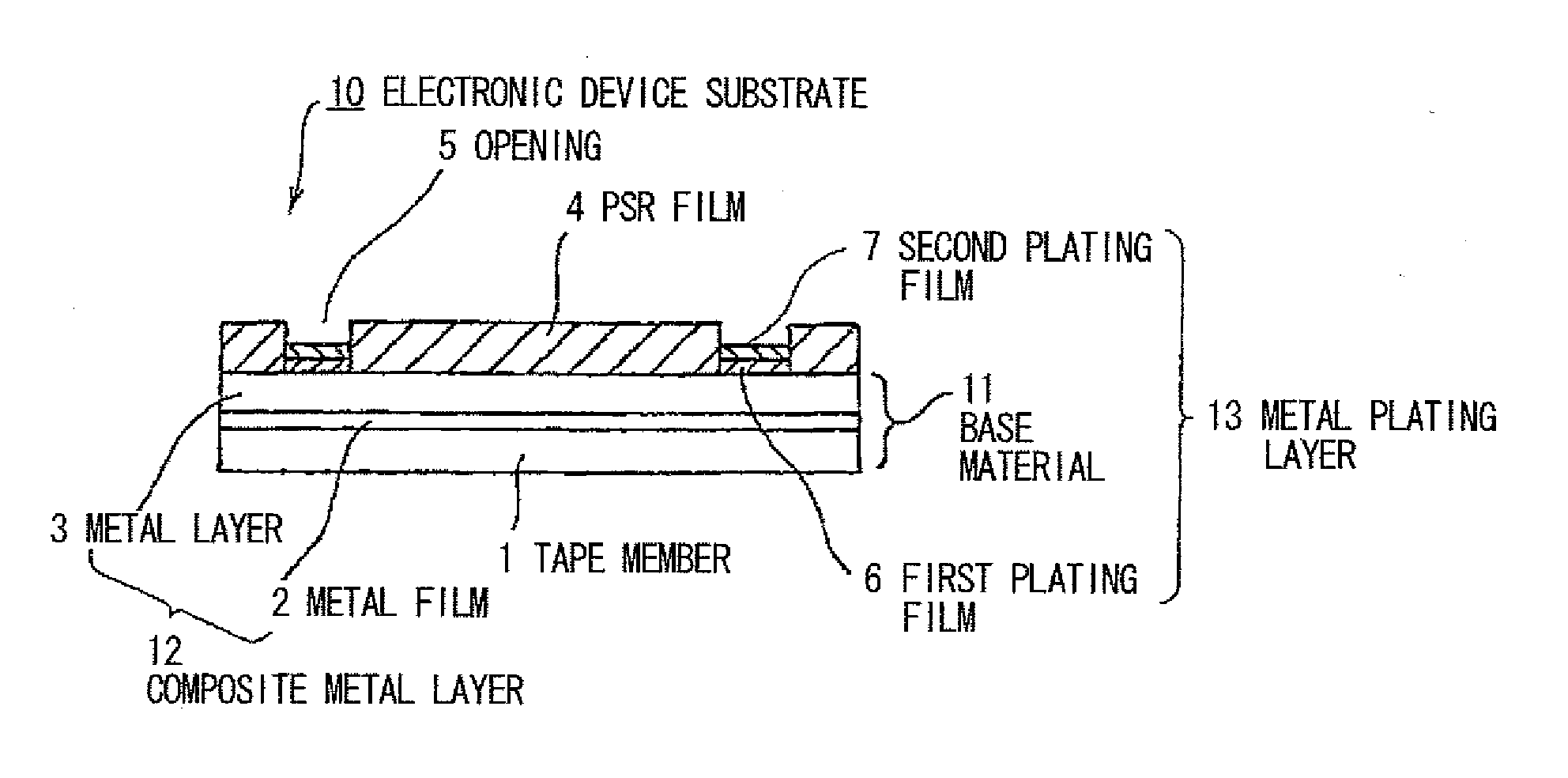
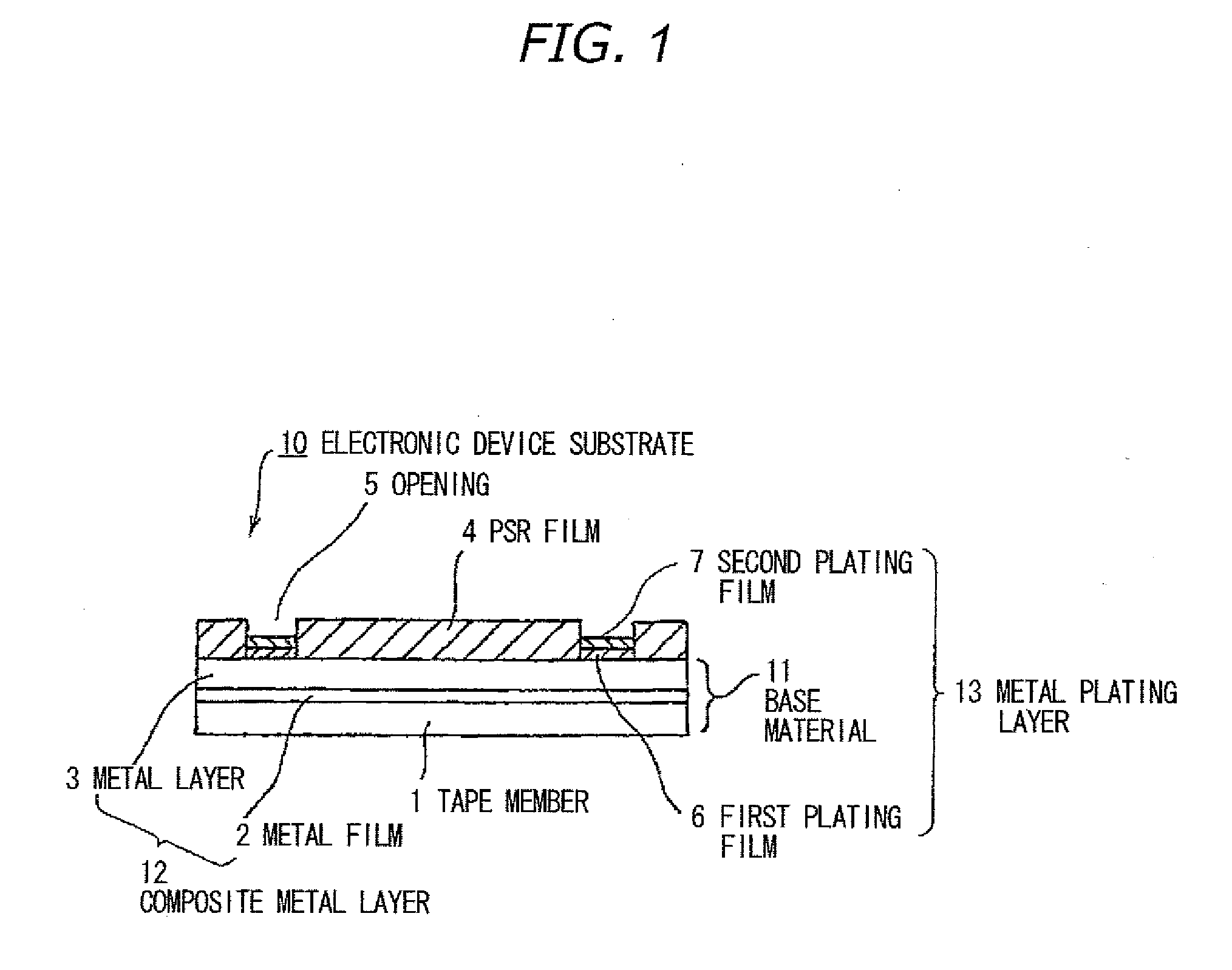
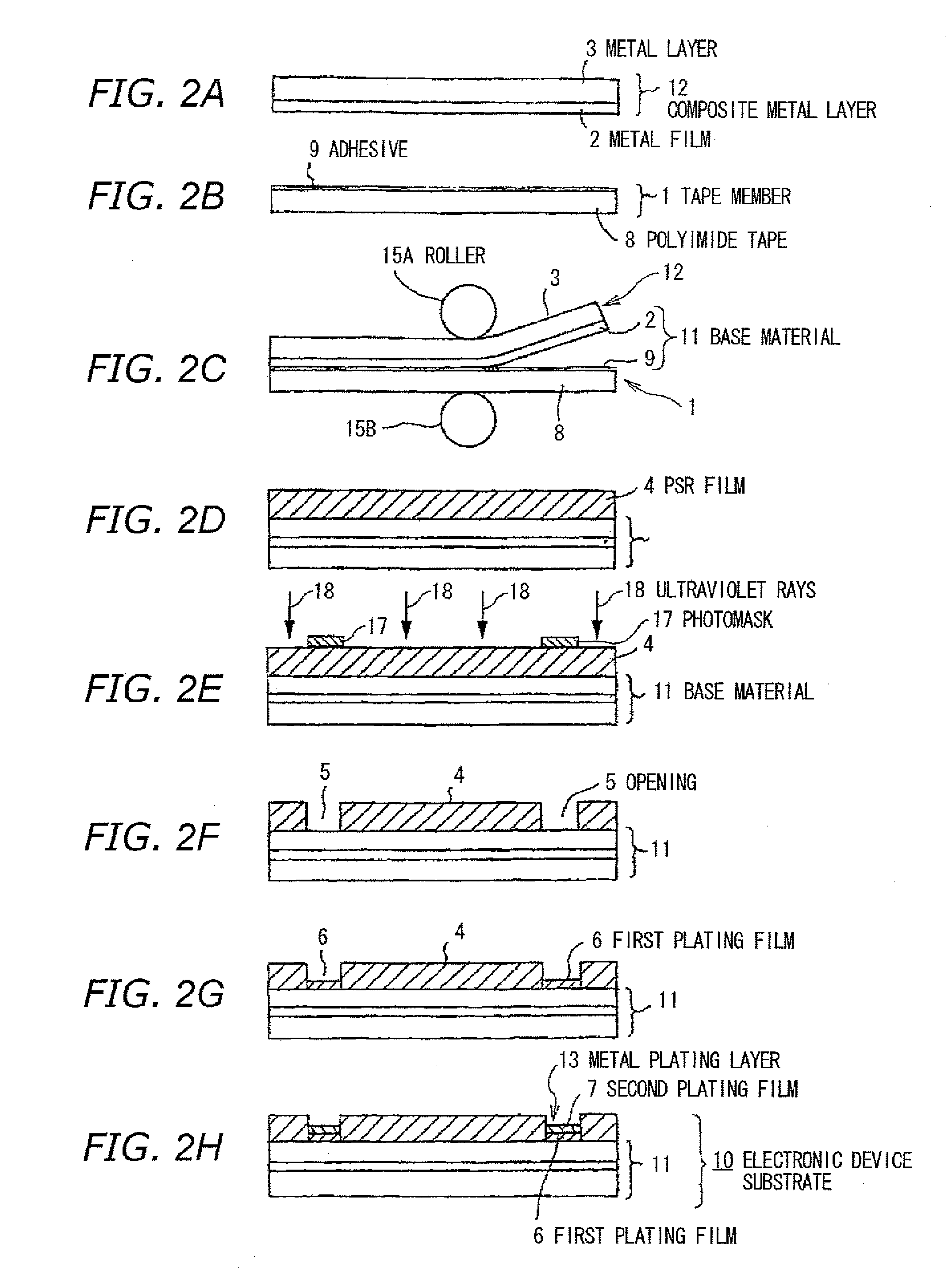
[0103]FIG. 1 shows an electronic device substrate in the first preferred embodiment according to the invention.

[0104]The electronic device substrate 10 comprises: a composite metal layer (or composite copper foil) 12 that a metal layer 3 formed of a copper-foil as a base material is provided with a release layer (not shown) formed thereon and a thin metal film 2 is formed on the release layer; a tape member 1 that is attached through an adhesive 9 (See FIG. 2B) to the composite metal layer 12; a PSR film 4 that is, as a first insulation layer, formed on an opposite surface of the metal layer 3 with a predetermined pattern; a first plating film 6 that is formed in an opening 5 formed at a predetermined position of the PSR film 4; and a second plating film 7 that is formed on the first plating film 6.

[0105]The metal layer 3 is desirably formed of a copper foil due to its availability, cost, high electrical conductivity, removal easiness ...

second embodiment

Composition of Electronic Device

[0126]FIG. 3 is a cross sectional view showing an electronic device substrate in the second preferred embodiment according to the invention.

[0127]The electronic device 20 comprises: an electronic device substrate 10′ that is formed by removing the base material 11 from the electronic device substrate 10 of the first embodiment; an electronic parts 21 mounted at a predetermined position on the electronic device substrate 10′; bonding wires 22 that connects an external connection terminal (not shown) on the electronic parts 21 to the second plating film 7 of the electronic device substrate 10′; a sealing resin 23, as insulating covering material, formed on the electronic device substrate 10′ to cover the electronic parts 21, the bonding wires 22 and the second plating film 7; a protruding terminal 24 formed on the back surface of the PSR film 4 and contacting the first plating film 6; and a surface treatment film 25 formed on the surface of the protrudi...

third embodiment

Composition of Electronic Device

[0147]FIG. 5 is a cross sectional view showing an electronic device substrate in the third preferred embodiment according to the invention.

[0148]The electronic device 30 comprises: an electronic device substrate 10′ that is formed by removing the base material 11 from the electronic device substrate 10 of the first embodiment; an electronic parts 21 mounted at a predetermined position on the electronic device substrate 10′; bonding wires 22 that connects an external connection terminal (not shown) on the electronic parts 21 to the second plating film 7 of the electronic device substrate 10′; a sealing resin 23, as insulating covering material, formed on the electronic device substrate 10′ to cover the electronic parts 21, the bonding wires 22 and the second plating film 7; a conductor wiring layer (or conductor circuit) 31 formed on the back surface of the PSR film 4 and contacting the first plating film 6; a surface treatment film 32 formed on the su...


PUM

PropertyMeasurementUnit
thicknessaaaaaaaaaa
thicknessaaaaaaaaaa
thickaaaaaaaaaa

Abstract

An electronic device substrate having: a base material formed of a thin board; an electrical insulation layer formed on the base material and having plural openings in a thickness direction thereof; and a metal plating layer filled in the plural openings. The base material has a metal layer, a release layer formed contacting the metal layer, and a metal film formed contacting the release layer.

Description

CROSS REFERENCE TO RELATED APPLICATION[0001]The present application is a divisional application of U.S. patent application Ser. No. 11 / 645,948 dated Dec. 27, 2006, which is based on Japanese patent application No. 2006-141862, the entire contents of which are incorporated herein by reference.BACKGROUND OF THE INVENTION[0002]1. Field of the Invention[0003]This invention relates to an electronic device substrate, an electronic device and methods for making the same and, in particular, to an electronic device that, despite having a coreless type structure advantageous to thinning or downsizing, is less likely to have a crack during its production process and has a structure advantageous for external mounting and a method of making the same. Also, this invention relates to an electronic device substrate used for the electronic device and a method of making the same.[0004]2. Description of the Related Art[0005]FIGS. 8A and 8B are a cross sectional view and a top view (mounting surface), ...

Claims


Application Information

Patent Timeline
Patent Type & Authority Applications(United States)
IPC IPC(8): H05K7/00H05K3/46
CPCH01L21/4832Y10T29/4913H01L23/3121H01L23/49582H01L24/45H01L2221/68345H01L2224/45144H01L2224/48227H01L2224/48228H01L2224/49171H01L2224/85439H01L2224/85444H01L2224/85464H01L2924/01004H01L2924/01046H01L2924/0105H01L2924/01078H01L2924/01079H01L2924/14H01L2924/15311H01L2924/19041H05K3/0023H05K3/007H05K3/06H05K3/243H05K3/284H05K2203/0156H05K2203/0571H05K2203/1469H01L21/568Y10T29/49155H01L2224/48465H01L2924/01028H01L2924/01013H01L2924/01067H01L2924/01019H01L24/49H01L24/48H01L2924/00014H01L2924/00H01L2224/05553H01L2224/48639H01L2224/48644H01L2224/48664H01L2924/10161H01L2924/181H01L2924/00012A43B5/025A43B13/186B29D35/142
Inventor MIYAMOTO, NOBUAKICHINDA, AKIRAHIRASAWA, KOKIUCHIDA, KENJI
Owner RENESAS ELECTRONICS CORP
Why Eureka
Try Eureka