Imaging device and method of driving solid state imaging element

a solid-state imaging and imaging element technology, applied in the direction of television system scanning details, radio control devices, television systems, etc., can solve the problems of inability to execute linearity corrections simply based on correction information, process cannot catch up with the signals that are being output from solid-state imaging elements sequentially, etc., to prevent the generation of residual charges in the connecting portion, improve the accuracy of decision making, and prevent lag

Active Publication Date: 2010-01-07
FUJIFILM CORP
View PDF5 Cites 16 Cited by
  • Summary
  • Abstract
  • Description
  • Claims
  • Application Information

AI Technical Summary

Benefits of technology

[0023]According to this configuration, the potential of the connecting portion is stable at a point of time the power supply is turned on. Therefore, decision accuracy can be improved by deciding the potential at a time when the power supply is turned on.
[0024]According to this configuration, the potential of the connecting portion is varied depending upon a used time of the imaging device. Therefore, generation of the residual charges in the connecting portion can be always prevented by deciding the potential every predetermined time period.
[0025]According to the present invention, it is possible to prevent the lag and also allow the linearity correction by preventing such a situation that the charges remain in the connecting portion between the photoelectric converting element and the semiconductor substrate, in an imaging device that is equipped with the solid state imaging element containing the photoelectric converting element provided over the semiconductor substrate.

Problems solved by technology

Therefore, if the samplings of signals are executed at such time interval, the process cannot catch up with the signals that are being output from the solid state imaging element sequentially.
As a result, a signal output is not decided uniquely in response to a quantity of incident light, and thus it is impossible to execute a linearity correction simply based on the correction information that are held in advance.

Method used


Image

  • Imaging device and method of driving solid state imaging element
  • Imaging device and method of driving solid state imaging element
  • Imaging device and method of driving solid state imaging element

Examples


first embodiment

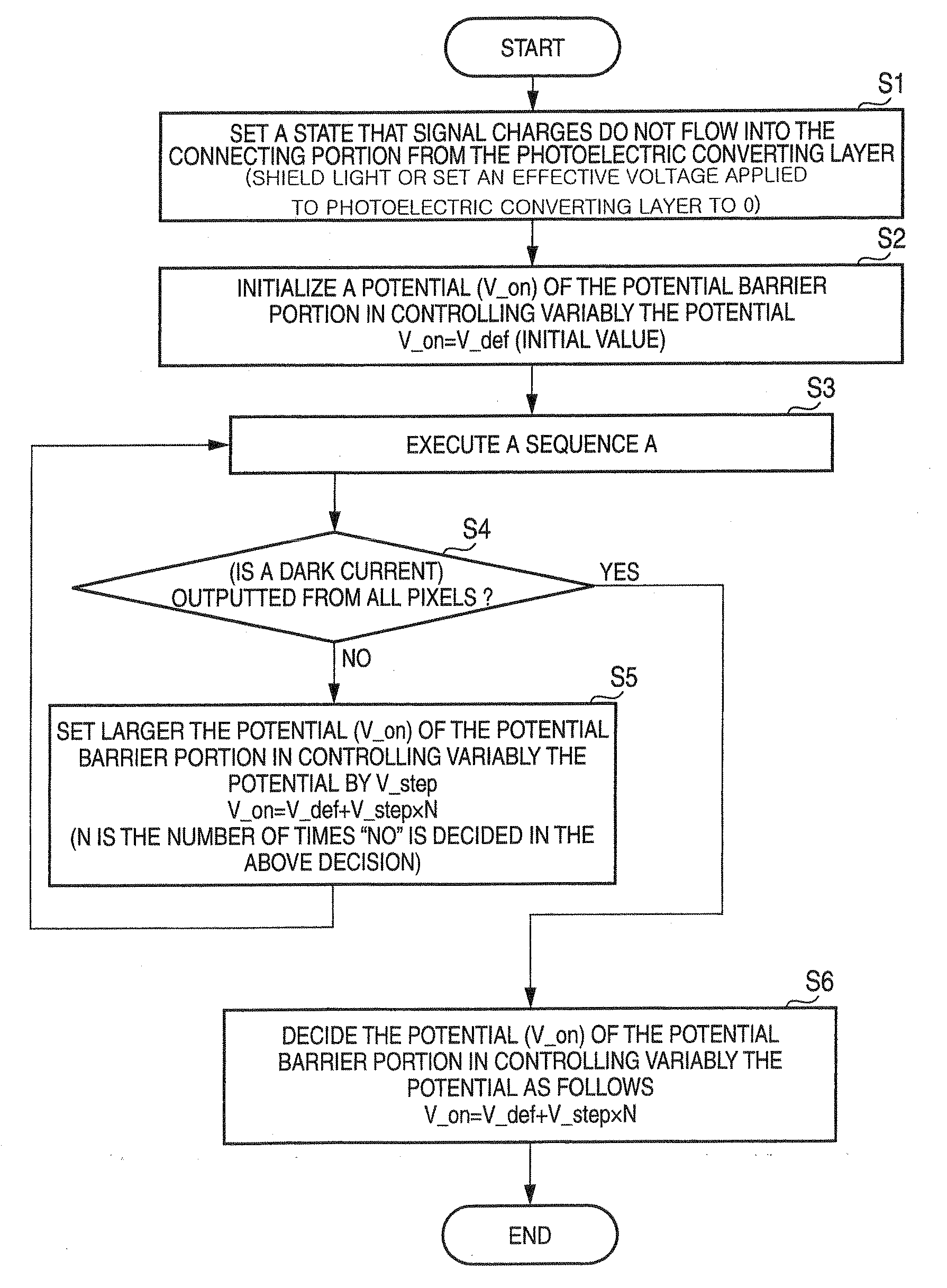
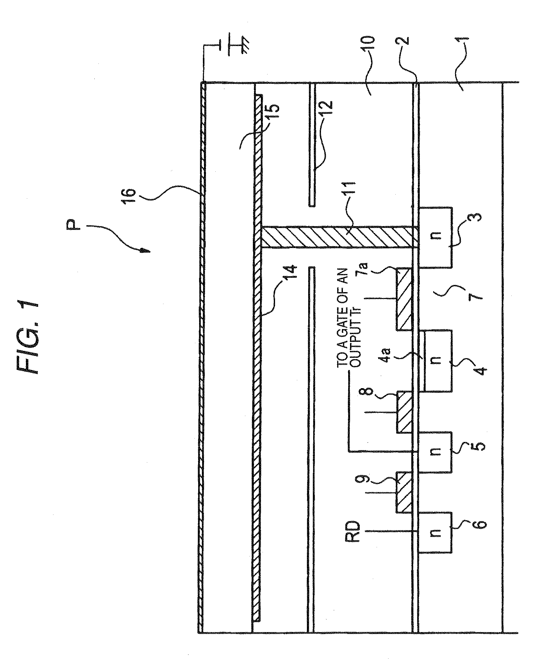
[0037]FIG. 1 is a schematic sectional view showing one pixel of a solid state imaging element as a first embodiment of the present invention. The solid state imaging element is constructed by arranging one pixel shown in FIG. 1 in plural on the same plane one-dimensionally or two-dimensionally. While taking as an example such a configuration that one pixel shown in FIG. 1 is aligned two-dimensionally in the row (horizontal) direction and the column (vertical) direction perpendicular to the row (horizontal) direction, explanation will be made hereunder.

[0038]The solid state imaging element shown in FIG. 1 contains a p-type silicon substrate 1 as a semiconductor substrate (referred to as a “substrate 1” hereinafter), and a photoelectric converting element P stacked over the substrate 1 via a gate insulating film 2 and an insulating layer 10.

[0039]The photoelectric converting element P is constructed to includes a lower electrode 14 formed on the insulating layer 10, a photoelectric co...

second embodiment

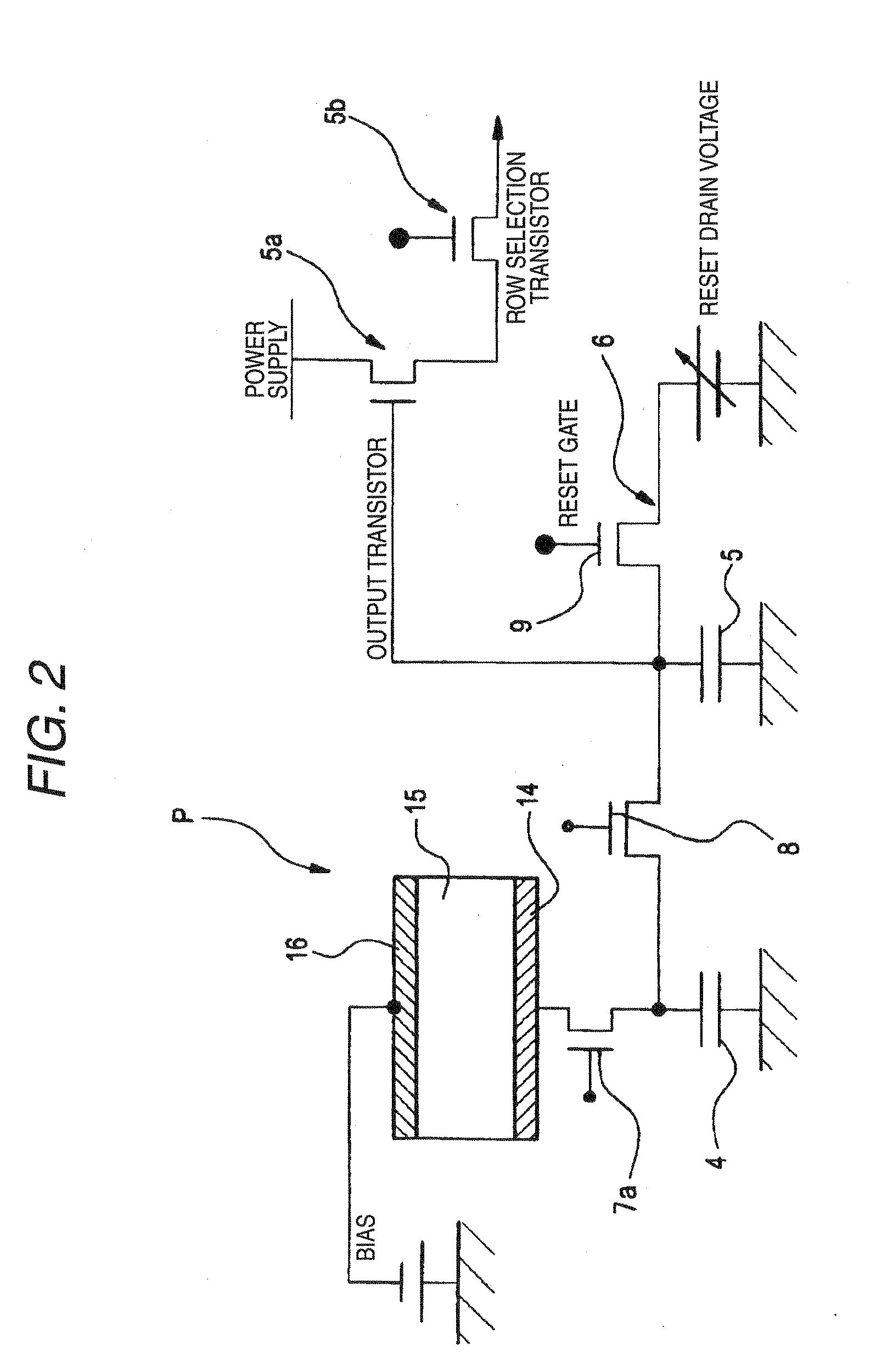
[0094]In the first embodiment, the reset noise can be eliminated exactly by accumulating temporarily the charges generated in the exposure period in the first charge accumulating portion 4. However, when an accuracy in eliminating the reset noise is not requested, the driving system in the first embodiment can be employed even in the configuration in which the first charge accumulating portion 4 is not provided.

[0095]The solid state imaging element that is installed into the imaging device of the second embodiment may be constructed by replacing the transfer gate 8 with the reset gate 9, replacing the second charge accumulating portion 5 with the reset drain 6, and connecting the gate of the output transistor to the first charge accumulating portion 4, in the solid state imaging elements shown in FIG. 1. Here, in the case of such configuration, the p-type impurity layer 4a formed on the surface of the first charge accumulating portion 4 should be deleted.

[0096]An operation of the im...


PUM


Abstract

An imaging device includes a solid state imaging element that includes a plurality of pixels; and a driving unit; wherein each pixel includes: a photoelectric converting element includes a pair of electrodes stacked above a semiconductor substrate and a photoelectric converting layer arranged between the electrodes; a connecting portion that is arranged in the semiconductor substrate; a potential barrier portion; a first charge accumulating portion; and a signal output circuit, and wherein the driving unit executes such a same potential driving that the connecting portion and the potential barrier portion are set to have a same potential by varying the potential of the potential barrier portion.

Description

[0001]The present application claims priority from Japanese Patent Application No. 2008-174320 filed on Jul. 3, 2008, the entire content of which is incorporated herein by reference.BACKGROUND[0002]1. Technical Field[0003]The present invention relates to an imaging device that is equipped with a solid state imaging element containing a plurality of pixels that have a photoelectric converting element, which has a pair of electrodes stacked over a semiconductor substrate and a photoelectric converting layer put between the electrodes, respectively.[0004]2. Description of the Related Art[0005]In JP-A-2005-268477, the solid state imaging element equipped with a semiconductor substrate on a signal reading circuit composed of MOS transistor circuits is formed, a photoelectric converting film stacked on the semiconductor substrate to generate charges in response to a quantity of incident light, a connecting portion which is provided on a surface of the semiconductor substrate and to which ...

Claims


Application Information

Patent Timeline
Patent Type & Authority Applications(United States)
IPC IPC(8): H04N5/335H01L27/146H04N5/357H04N5/363H04N5/369H04N5/374H04N5/378
CPCH01L27/14621H01L27/14632H01L27/14643H04N5/374H04N5/3559H04N5/3575H04N5/3597H01L27/14654H04N25/59H04N25/626H04N25/616H04N25/76
Inventor OTA, MOTOARI
Owner FUJIFILM CORP
Why Eureka
Try Eureka