Memory device and device and method for detecting motion vector

a technology of motion vector and memory device, which is applied in the field of memory device and a device and a device for detecting motion vector, can solve the problems of vector detection circuit b>200/b> having a disadvantage of higher costs, the inability to increase the computing speed, and the disadvantage of increasing the cos

Inactive Publication Date: 2010-01-07
SONY CORP
View PDF4 Cites 10 Cited by
  • Summary
  • Abstract
  • Description
  • Claims
  • Application Information

AI Technical Summary

Benefits of technology

[0037]It is an object of the present invention to provide a memory device that enables simultaneous processing of data reading and computing, to improve a computing speed and reduce costs due to a decrease in number of the computing units.
[0038]It is another object of the present invention to provide a memory device that can obtain difference data between pixel data of a first frame and that of a second frame speedily and inexpensively.
[0039]It is a further object of the present invention to provide a memory device that can obtain added-up data of plural items of data speedily and inexpensively.

Problems solved by technology

Therefore, this method of reading the items of data and performing the operations sequentially leads to a disadvantage that a computing speed cannot be increased.
Further, since the computing unit is necessary separately from the memory block 300, costs are increased by that much disadvantageously.
The above motion vector detection circuit 200 has had a disadvantage of higher costs due to a necessity of the circuits for computing difference data, an absolute value, a total sum, etc. as arithmetic circuits.

Method used


Image

  • Memory device and device and method for detecting motion vector
  • Memory device and device and method for detecting motion vector
  • Memory device and device and method for detecting motion vector

Examples


Embodiment Construction

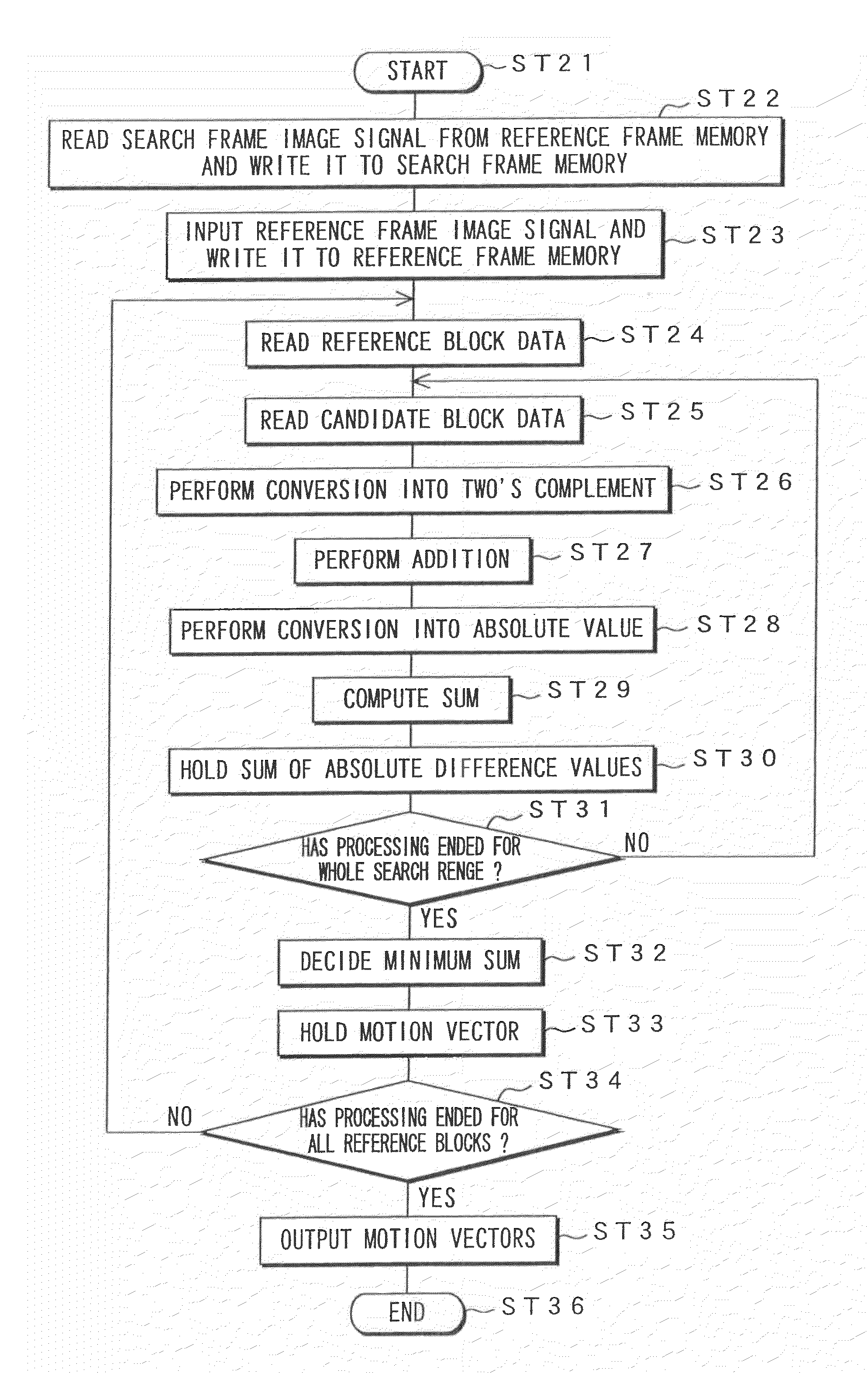
[0093]The following will describe embodiments of the present invention with reference to drawings.

[0094]FIG. 5 shows a configuration of motion-compensation-predictive-encoding device 100 according to an embodiment.

[0095]This encoding device 100 has an input terminal 101 to which an image signal Di is input, a subtracter 102 for computing a difference between the image signal Di supplied to this input terminal 101 and a predictive image signal supplied from a later-described motion compensation circuit 110, a DCT circuit 103 for performing discrete cosine transformation (DCT) on a difference signal obtained at this subtracter 102, a quantization circuit 104 for quantizing a DCT coefficient obtained at this DCT circuit 103, and an output terminal 105 for outputting an encoded signal Do obtained at this quantization circuit 104.

[0096]The encoding device 100 further has an inverse quantization circuit 106 for inverse-quantizing the encoded signal Do obtained at the quantization circuit ...


PUM


Abstract

This invention relates to a memory device and the like that are preferably applied to a case where motion vector is detected using a block matching. Pixel data of a first frame (a reference frame) is stored in a unit A of memory cell array portion 20a in straight binary format. Pixel data of a second frame (a search frame) is stored in a unit B of memory cell array portion 20b in two's complement format. The units A and B have a plurality of memory cells, respectively. Word lines WL related to the pixel data of the first and second frames are simultaneously activated so that charges accumulated in capacitors of each of the memory cells can be combined along one bit line BL. A / D converter 53 outputs a digital signal (absolute difference value) having a value that corresponds to a total amount of charges. When reading the pixel data, a subtraction and a conversion into the absolute difference value are simultaneously performed.

Description

CROSS-RELATED TO RELATED APPLICATIONS[0001]This application is a divisional of U.S. patent application Ser. No. 10 / 531,005, filed on Apr. 12, 2005, the entire content of which is incorporated herein by reference. U.S. patent application Ser. No. 10 / 531,005 is the National Stage of PCT / JP03 / 13204, filed on Oct. 15, 2003, which claims priority to Japanese Application No. 2002-300902, filed on Oct. 15, 2002 and Japanese Application No. 2002-300903, filed on Oct. 15, 2002.TECHNICAL FIELD[0002]The present invention relates to a memory device and a device and method for detecting a motion vector.[0003]More specifically, it relates to a memory device having a configuration for activating a plurality of word lines simultaneously to combine, along one bit line, charges accumulated in capacitors of a plurality of memory cells connected to this plurality of word lines and output a digital signal having a value that corresponds to a total amount of these charges so that data can be read and com...

Claims


Application Information

Patent Timeline
Patent Type & Authority Applications(United States)
IPC IPC(8): H04N7/26G11C11/56H04N7/50
CPCG06T7/202G06T2200/28G06T2207/10016G11C7/1006H04N19/436H04N5/145H04N19/51H04N19/61H04N19/43G11C11/565G06T7/231H04N19/433
Inventor KONDO, TETSUJIRONIITSUMA, WATARUKOBAYASHI, NAOKI
Owner SONY CORP
Why Eureka
Try Eureka