Light-emitting diode package

a technology of light-emitting diodes and packages, applied in the field of light sources, can solve the problems of not being suitable for illuminating distant objects, etc., and achieve the effect of reducing the light-emitting angle of the second surface of the lens

Active Publication Date: 2010-01-14
HIMAX DISPLAY INC
View PDF6 Cites 41 Cited by
  • Summary
  • Abstract
  • Description
  • Claims
  • Application Information

AI Technical Summary

Benefits of technology

[0010]In the LED package according to the embodiments of the present invention, since the gap is formed between the LED chip and the lens and has different refractive index from that of the lens, and since the lens has the protrusion and the protruding ring, the range of the light emitting angle of the light from the second surface of the lens is reduced.

Problems solved by technology

However, referring to FIGS. 1 and 2, the range of the light emitting angle θ1 and θ2 of the conventional LED packages 100 and 200 is large, approximate to 180 degrees, such that the LED packages 100 and 200 are not suitable for illuminating distant objects.

Method used


Image

  • Light-emitting diode package
  • Light-emitting diode package
  • Light-emitting diode package

Examples


first embodiment

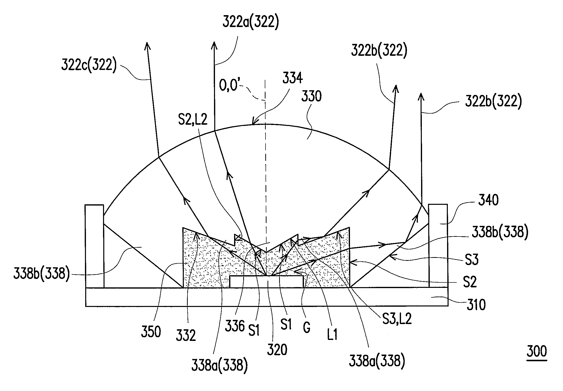
[0021]FIG. 3A is a schematic cross-sectional view of a light-emitting diode (LED) package according to a first embodiment of the present invention, and FIG. 3B is a schematic bottom view of a lens in FIG. 3A. Referring to FIGS. 3A and 3B, the LED package 300 of the present embodiment includes a carrier 310, a LED chip 320, and a lens 330. The LED chip 320 is disposed on the carrier 310. In the present embodiment, the carrier 310 is, for example, a circuit substrate. However, in other embodiment (not shown), the carrier may be a lead frame or other appropriate carrier. The lens 330 is disposed on the carrier 310 and above the LED chip 320. In the present embodiment, the LED package 300 further includes a supporter 340 disposed around the LED chip 320 and connecting the carrier 310 and the lens 330 for supporting the lens 330. A gap G is formed between the LED chip 320 and the lens 330. In the present embodiment, a minimum distance between the lens 330 and the LED chip 320 is greater ...

second embodiment

[0027]FIG. 4A is a schematic cross-sectional view of an LED package according to a second embodiment of the present invention, and FIG. 4B is a schematic bottom view of a lens in FIG. 4A. Referring to FIGS. 4A and 4B, the LED package 300′ is similar to the above LED package 300 in FIG. 3A, but the differences therebetween are as follows. In the LED package 300′, the first part of the beam 322a passes through the first subsurface S1 and the second surface 334 in sequence. In addition, a second part of the beam 322b′ passes through a second subsurface S2′ of each protruding ring 338′ of a lens 330′ and the second surface 334 thereof in sequence. Moreover, a third part of the beam 322c′ passes through the third subsurface S3′ of each protruding ring 338′ and the second surface 334 in sequence. In other words, there occurs no TIR on the protruding ring 338′.

third embodiment

[0028]FIG. 5A is a schematic cross-sectional view of an LED package according to a third embodiment of the present invention, and FIG. 5B is a schematic bottom view of a lens in FIG. 5A. Referring to FIGS. 5A and 5B, the LED package 300″ of the present embodiment is similar to the above LED package 300′ in FIG. 4A, but the differences therebetween are as follows. In the LED package 300″, a protrusion 336″ has a first subsurface S1″, and each of the protruding rings 338″, such as the protruding rings 338a″ and 338b″, has a second subsurface S2″ surrounding the first subsurface S1″. Any one cross-section of the first subsurface S1″ formed by cutting the lens 330″ along the optical axis O″ of the beam 322″ is a first curved line C1, and any one cross-section of the second subsurfaces S2″ of the protruding rings 338″ formed by cutting the lens 330″ along the optical axis O″ of the beam 322″ includes a second curved line C2, a third curved line C3, a fourth curved line C4, and a fifth cu...


PUM


Abstract

An LED package including a carrier, a LED chip, and a lens is provided. The LED chip is disposed on the carrier. The lens is disposed on the carrier and above the LED chip. A gap is formed between the LED chip and the lens. The lens has a first surface, a second surface, a protrusion, and at least one protruding ring. The first surface faces the LED chip. The second surface is opposite to the first surface. The protrusion is located at the first surface. The protruding ring is located at the first surface and surrounds the protrusion.

Description

BACKGROUND OF THE INVENTION[0001]1. Field of the Invention[0002]The present invention generally relates to a light source and, in particular, to a light-emitting diode (LED) package.[0003]2. Description of Related Art[0004]As the luminous efficiency of light emitting diodes (LEDs) is increasingly improved, LEDs have replaced fluorescent lamps and incandescent lamps in some fields, for example, lamps of scanners requiring for quick response, lamps of projection apparatus, backlight sources or front light sources of liquid crystal displays (LCDs), illumination for dashboards of automobiles, traffic lights, common illumination devices, etc. Compared with conventional lamps, the LEDs have absolute advantages, for example, small volume, long lifespan, low driving voltage / current, non-fragile, mercury free (no pollution), and good luminous efficiency (power saving).[0005]FIG. 1 is a schematic structural view of a conventional LED package. Referring to FIG. 1, the conventional LED package ...

Claims


Application Information

Patent Timeline
Patent Type & Authority Applications(United States)
IPC IPC(8): H01L33/00
CPCH01L33/54G02B19/0061G02B19/0028H01L33/58H01L2924/181H01L2224/48091H01L2224/48247H01L2924/00014H01L2924/00012
Inventor CHEN, CHUN-MIN
Owner HIMAX DISPLAY INC
Why Eureka
Try Eureka