Semiconductor device and method of manufacturing the same

a semiconductor and semiconductor technology, applied in the direction of semiconductor devices, electrical devices, transistors, etc., can solve the problems of difficult etching, expose the substrate, and difficult to remove hf contained films by etching. , to achieve the effect of difficult etching

Inactive Publication Date: 2010-01-14
RENESAS ELECTRONICS CORP
View PDF7 Cites 19 Cited by
  • Summary
  • Abstract
  • Description
  • Claims
  • Application Information

AI Technical Summary

Benefits of technology

[0013]According to the present invention, even though transistors have the same conductive type, the transistors can be made to have preferable characteristics in accordance with a utilization purpose.

Problems solved by technology

According to the examination result of the present inventor, when a process of exposing the substrate to the bottom portion of the second trench is executed, if the Hf contained film is formed on the substrate, it is difficult to remove the Hf contained film by etching and expose the substrate.
Since the heat treatment is performed when the impurities are implanted into the substrate to form the source / drain region, crystallization of Hf in the Hf contained film is progressed, and it becomes difficult to remove the Hf contained film by etching.
In particular, when the Hf contained film does not contain Si, etching becomes difficult.

Method used


Image

  • Semiconductor device and method of manufacturing the same
  • Semiconductor device and method of manufacturing the same
  • Semiconductor device and method of manufacturing the same

Examples


first embodiment

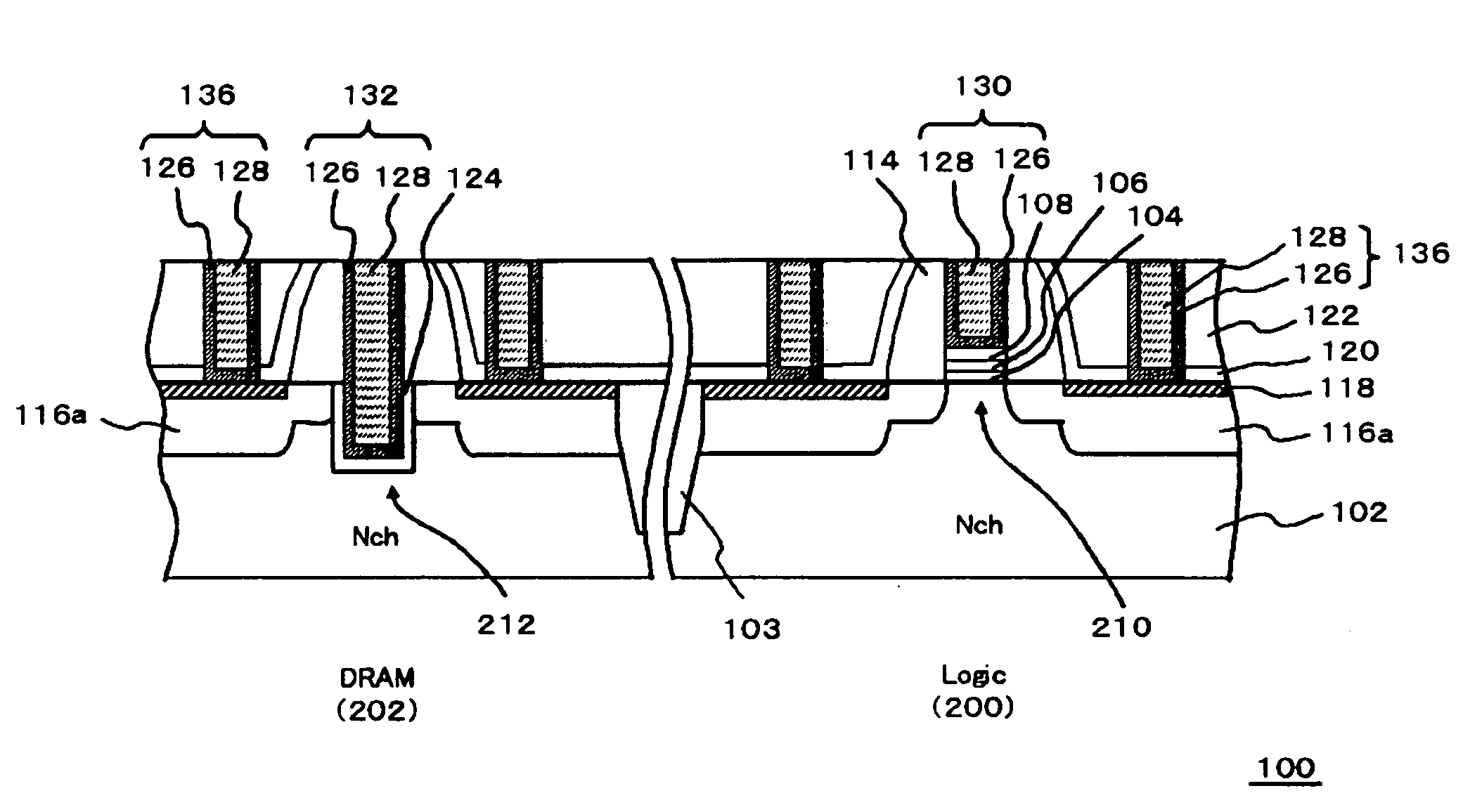
[0032]FIG. 1 is a cross-sectional view illustrating the configuration of a semiconductor device 100 according to this embodiment.

[0033]The semiconductor device 100 (substrate) includes a semiconductor substrate 102 where a logic region 200 (described as Logic in the drawings) and a Dynamic Random Access Memory (DRAM) region 202 (described as DRAM in the drawings) serving as a memory region are formed. The semiconductor substrate 102 is, for example, a silicon substrate.

[0034]The semiconductor device 100 includes first and second transistors 210 and 212 that are formed on the semiconductor substrate 102 and have the same conductive type. The first transistor 210 is formed in the logic region 200. The second transistor 212 is formed in the DRAM region 202. In this embodiment, the first transistor 210 includes an Hf contained gate insulating film 106 (Hf contained film) as a gate insulating film. Meanwhile, the second transistor 212 includes a silicon oxide film 124 as a gate insulatin...

second embodiment

[0068]FIG. 10 is a cross-sectional view illustrating the configuration of a semiconductor device 100 according to this embodiment.

[0069]The second embodiment is different from the first embodiment in that the second gate electrode 132 of the second transistor 212 is not formed in the semiconductor substrate 102.

[0070]Next, referring to FIGS. 11A to 14, a sequence of manufacturing the semiconductor device 100 according to this embodiment will be described. FIGS. 11A to 14 are process cross-sectional views illustrating a sequence of manufacturing a semiconductor device 100 according to this embodiment. In the following description, the case where the first transistor 210 and a third transistor 214 that has a conductive type opposite to that of the first transistor 210 are formed in the logic region 200 is exemplified.

[0071]Even in this embodiment, since the sequence that is described with reference to FIGS. 2A to 5B is the same as that of the first embodiment, the description thereof ...


PUM


Abstract

A semiconductor device, including: a first transistor formed on a substrate and including an Hf contained film as its gate insulating film; and a second transistor formed on said substrate and having the same conductive type as that of said first transistor, said second transistor including a silicon oxide film and not including an Hf contained film as its gate insulating film is provided.

Description

[0001]This application is based on Japanese patent application NO. 2008-179601, the content of which is incorporated hereinto by reference.BACKGROUND[0002]1. Technical Field[0003]The present invention relates to a semiconductor device and a method of manufacturing the semiconductor device.[0004]2. Related Art[0005]In recent years, as a material that constitutes a semiconductor device, utilization of a high-dielectric-constant film called high-k has been examined. Representative examples of a high-k material may include oxides including Zr and Hf. If these materials are used for a gate insulating film of a MOSFET, a high-speed transistor can be realized. Japanese Unexamined patent publication NO. 2002-280461 discloses a CMOS device that includes an nMOSFET and a pMOSFET using the high-k material.[0006]Further, as a method of forming a metal gate, a gate-last (damascene gate) process that forms a gate electrode after forming a source / drain may be adopted. Japanese Unexamined patent pu...

Claims


Application Information

Patent Timeline
Patent Type & Authority Applications(United States)
IPC IPC(8): H01L27/088H01L21/8242
CPCH01L21/823456H01L21/823462H01L27/10897H01L27/10894H01L27/10814H10B12/315H10B12/50H10B12/09
Inventor MATSUBARA, YOSHIHISA
Owner RENESAS ELECTRONICS CORP
Why Eureka
Try Eureka