Liquid crystal display device and method for manufacturing the same

a liquid crystal display and liquid crystal technology, applied in non-linear optics, instruments, optics, etc., can solve the problems of uneven display defective operation, easy cracking of element formation layers including semiconductor elements, etc., to reduce the damage of liquid crystal display devices by local charging, reduce image quality, and reduce the effect of stress due to bending

Inactive Publication Date: 2010-01-14
SEMICON ENERGY LAB CO LTD
View PDF51 Cites 34 Cited by
  • Summary
  • Abstract
  • Description
  • Claims
  • Application Information

AI Technical Summary

Benefits of technology

[0019]When a conductive layer is formed over a surface of the first structure body or / and the second structure body to have a thickness through which light passes, damage to the liquid crystal display device by local charging can be reduced without causing a decrease in image quality.
[0020]The first structure body and the second structure body preferably have the same thickness. The first impact relaxation layer and the second impact relaxation layer also preferably have the same thickness. In addition, the total thickness of the first structure body and the first impact relaxation layer and the total thickness of the second structure body and the second impact relaxation layer are preferably larger than the total thickness of the element formation layer and a liquid crystal layer. In that case, the element formation layer and the liquid crystal layer are located in the middle of a cross section of the liquid crystal display device; thus, stress due to bending can be reduced.
[0021]A flexible liquid crystal display device which is not easily damaged even if subjected to external pressure can be obtained, and the reliability of a liquid crystal display device can be increased. In addition, a highly reliable liquid crystal display device which is not easily damaged even if subjected to external pressure can be manufactured with high yield.

Problems solved by technology

However, a substrate of a flexible liquid crystal display device has flexibility; thus, an element formation layer including semiconductor elements easily cracks by local pressure applied from the outside or by local linear pressure applied due to bending of the liquid crystal display device.
There are also problems caused by these, such as defective operation and uneven display of the liquid crystal display device.
In addition, the adhesion between the element formation layer and the flexible substrate is poor, and the flexible substrate is easily separated from the element formation layer.
Thus, there is a problem of low yield.

Method used


Image

  • Liquid crystal display device and method for manufacturing the same
  • Liquid crystal display device and method for manufacturing the same
  • Liquid crystal display device and method for manufacturing the same

Examples


embodiment 1

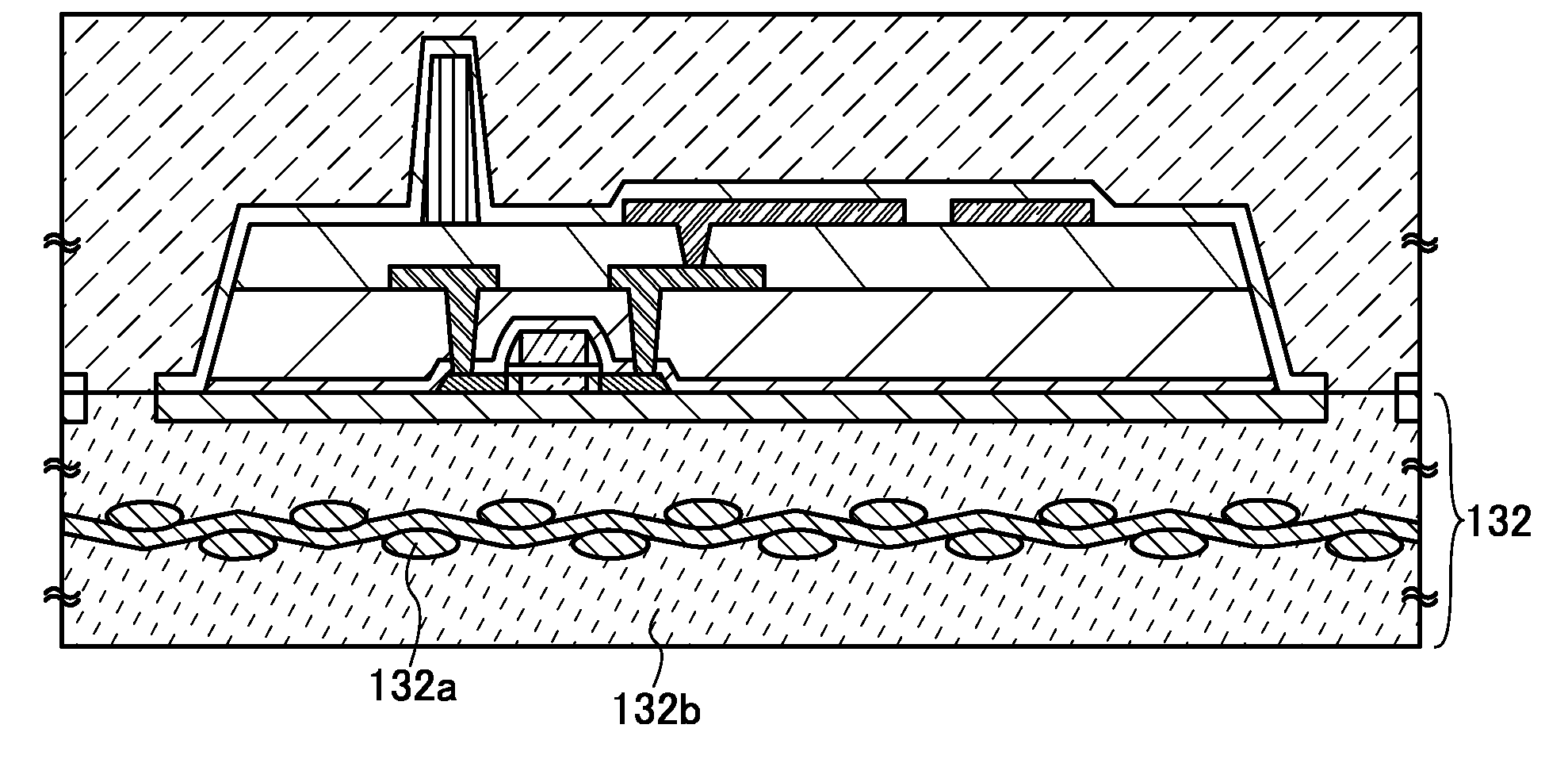
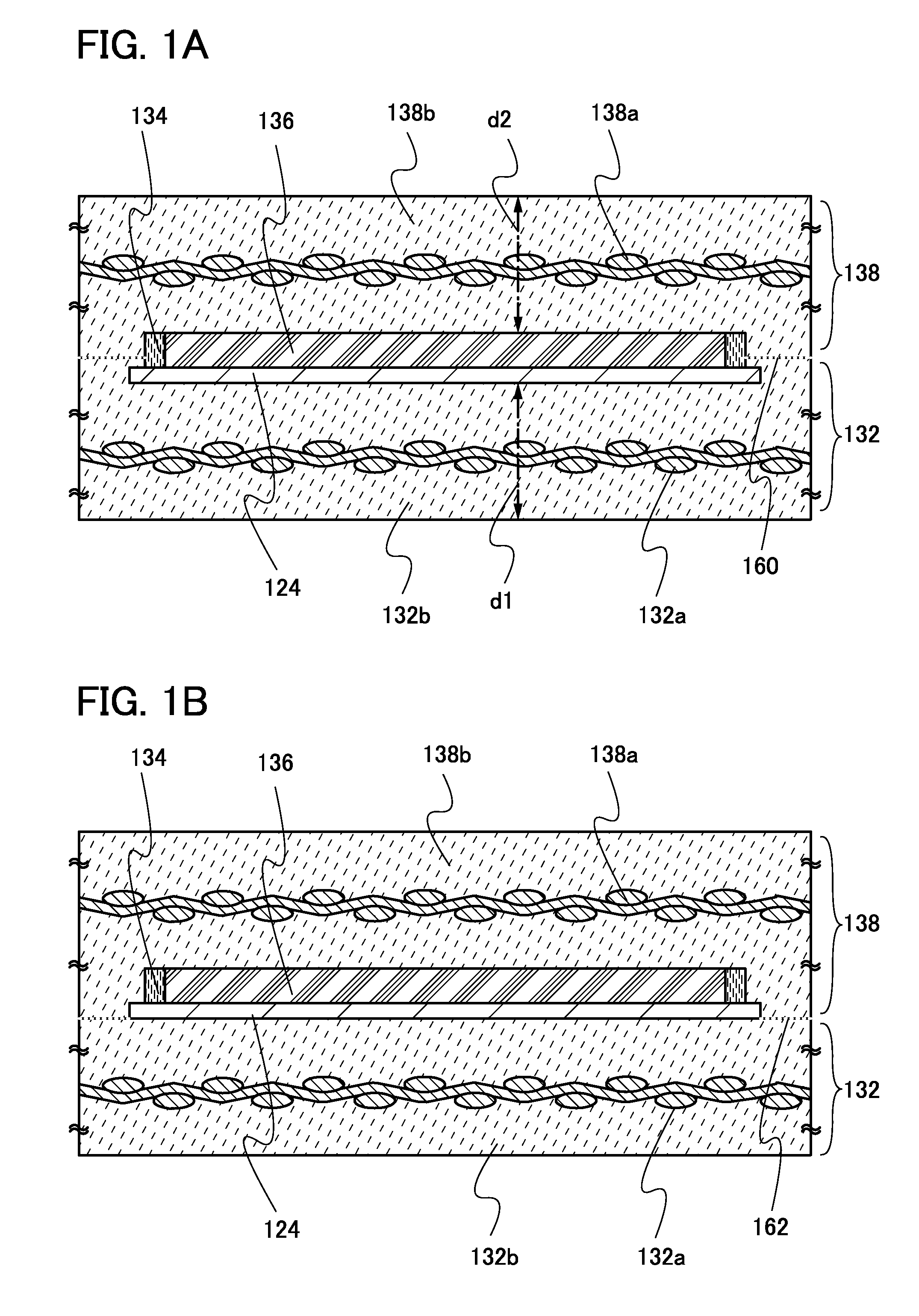
[0053]In this embodiment, a flexible and highly reliable liquid crystal display device which is not easily damaged by external pressure or bending is described with reference to FIGS. 1A and 1B.

[0054]A liquid crystal display device described in this embodiment has a liquid crystal layer 136, a first structure body 132 and a second structure body 138 facing each other with the liquid crystal layer 136 interposed therebetween, a seal member 134 for enclosing the liquid crystal layer 136, and an element formation layer 124 including a pixel electrode, a semiconductor element, a capacitor element, a wiring, and the like. A feature of the liquid crystal display device is that the first structure body 132 and the second structure body 138 are fixed in contact with each other outside the seal member 134 as indicated with a broken line 160 (see FIG. 1A). Note that the broken line 160 indicating a region where the first structure body 132 and the second structure body 138 are in close contac...

embodiment 2

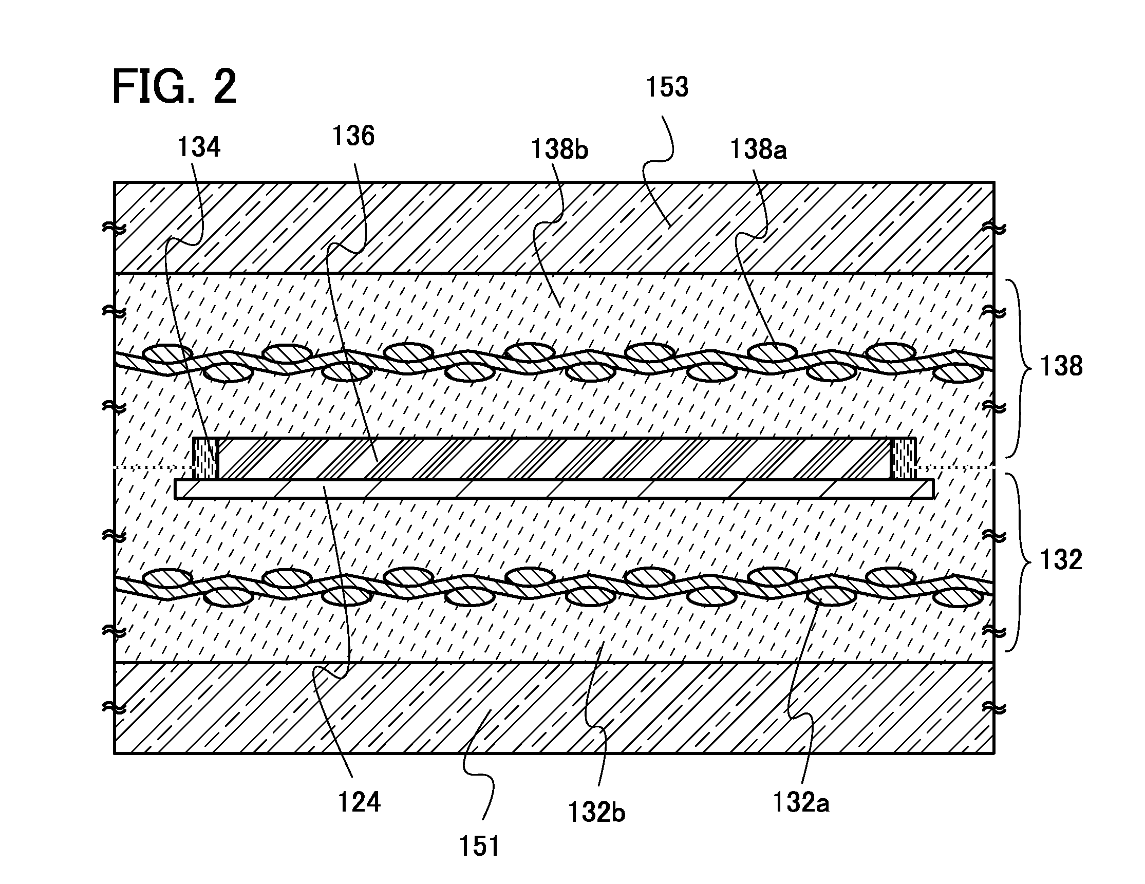
[0085]An object of this embodiment is to provide a liquid crystal display device which is not easily damaged even if subjected to planar pressure or linear pressure, and details are hereinafter described.

[0086]A liquid crystal display device described in this embodiment has a liquid crystal layer 136, a first structure body 132 and a second structure body 138 facing each other with the liquid crystal layer 136 interposed therebetween, a seal member 134 for enclosing the liquid crystal layer 136, and an element formation layer 124 including a pixel electrode, a semiconductor element, a capacitor element, a wiring, and the like. A feature of the liquid crystal display device is to have a first impact relaxation layer 151 outside the first structure body 132 and to have a second impact relaxation layer 153 outside the second structure body 138.

[0087]The first impact relaxation layer 151 and the second impact relaxation layer 153 are effective in dispersing and weakening force that is a...

embodiment 3

[0094]An object of this embodiment is to reduce damage due to electrical stress such as static electricity to provide a highly reliable liquid crystal display device, and details are hereinafter described.

[0095]A feature of this embodiment is that a conductive layer is formed on the outermost surface of a liquid crystal display device.

[0096]A conductive layer 170 is formed on the outer surface of the first structure body 132 or the second structure body 138 (here, the first structure body 132 provided on the element formation layer 124 side). Note that when an impact relaxation layer is formed outside each of the first structure body 132 and the second structure body 138 as described in Embodiment 2, a conductive layer is formed on the outer surface of the impact relaxation layer.

[0097]The conductive layer 170 disperses static electricity that is to be applied to the liquid crystal display device due to electrostatic discharge or prevents local presence (localization) of charges (pr...


PUM

PropertyMeasurementUnit
thicknessaaaaaaaaaa
thicknessaaaaaaaaaa
thicknessaaaaaaaaaa

Abstract

A flexible and highly reliable liquid crystal display device which is not easily damaged even if subjected to external pressure is provided. A method for manufacturing, with high yield, a flexible and highly reliable liquid crystal display device which is not easily damaged even if subjected to external pressure is also provided. A liquid crystal display device including a first structure body including a first fibrous body and a first organic resin, a second structure body including a second fibrous body and a second organic resin, a liquid crystal interposed between the first and second structure bodies, and a seal member for fixing the first and second structure bodies and for enclosing the liquid crystal. The first and second fibrous bodies are impregnated with the first and second organic resins, respectively, and the first structure body and the second structure body are in contact with each other.

Description

BACKGROUND OF THE INVENTION[0001]1. Field of the Invention[0002]The present invention relates to a liquid crystal display device having flexibility and a method for manufacturing the liquid crystal display device.[0003]2. Description of the Related Art[0004]In recent years, technology for forming thin film transistors (TFTs) using a thin semiconductor film (with a thickness of about several tens of nanometers to several hundreds of nanometers) formed over a substrate having an insulating surface has been attracting attention. Thin film transistors are applied to a wide range of electronic devices such as ICs or electro-optical devices, and prompt development of thin film transistors that can be used as switching elements in display devices, in particular, is being pushed.[0005]Glass substrates and quartz substrates are often used as substrates of such display devices; however, there are disadvantages to using glass substrates and quartz substrates in that they are heavy as well as b...

Claims


Application Information

Patent Timeline
Patent Type & Authority Applications(United States)
IPC IPC(8): G02F1/1333G02F1/1339
CPCG02F1/133305G02F2202/22G02F2201/503
Inventor OIKAWA, YOSHIAKIEGUCHI, SHINGOMASHIYAMA, MITSUOKATANIWA, MASATOSHISHOJI, HIRONOBUNAKADA, MASATAKA
Owner SEMICON ENERGY LAB CO LTD
Why Eureka
Try Eureka