Particle Free Wafer Separation

a technology of wafers and wafers, applied in the direction of semiconductor/solid-state device manufacturing, basic electric elements, electric apparatus, etc., can solve the problems of particle generation, nano-scrubbing does not solve particle generation, bonding failure, etc., to reduce particle contamination, reduce yield, and reduce the effect of wafer bonding defects

Inactive Publication Date: 2010-01-14
TAIWAN SEMICON MFG CO LTD
View PDF6 Cites 20 Cited by
  • Summary
  • Abstract
  • Description
  • Claims
  • Application Information

AI Technical Summary

Benefits of technology

[0010]An advantage of a preferred embodiment of the present invention is the reduction in particles contamination that is an inherent part of many singulation processes. This reduction in particle contamination leads to fewer defects during wafer bonding, and, therefore, increases yield.

Problems solved by technology

Unfortunately, die sawing, in addition to possible delamination and destruction of the die, also generates particles as the saw cuts through the wafer.
These particles can then redeposit and contaminate the individual die, potentially causing bonding failures if the particles are larger than the bonding gap requirements (which may in some cases be less than 1 μm).
However, nano-scrubbing does not solve the problem of particles.
These particles may remain after singulation and may still interfere with subsequent bonding of the die to other devices, thereby driving down the overall yield of wafers.

Method used


Image

  • Particle Free Wafer Separation
  • Particle Free Wafer Separation
  • Particle Free Wafer Separation

Examples


Embodiment Construction

[0017]The making and using of the presently preferred embodiments are discussed in detail below. It should be appreciated, however, that the present invention provides many applicable inventive concepts that can be embodied in a wide variety of specific contexts. The specific embodiments discussed are merely illustrative of specific ways to make and use the invention, and do not limit the scope of the invention.

[0018]The present invention will be described with respect to preferred embodiments in a specific context, namely singulating a semiconductor die from a semiconductor wafer. The invention may also be applied, however, to other wafer separation processes.

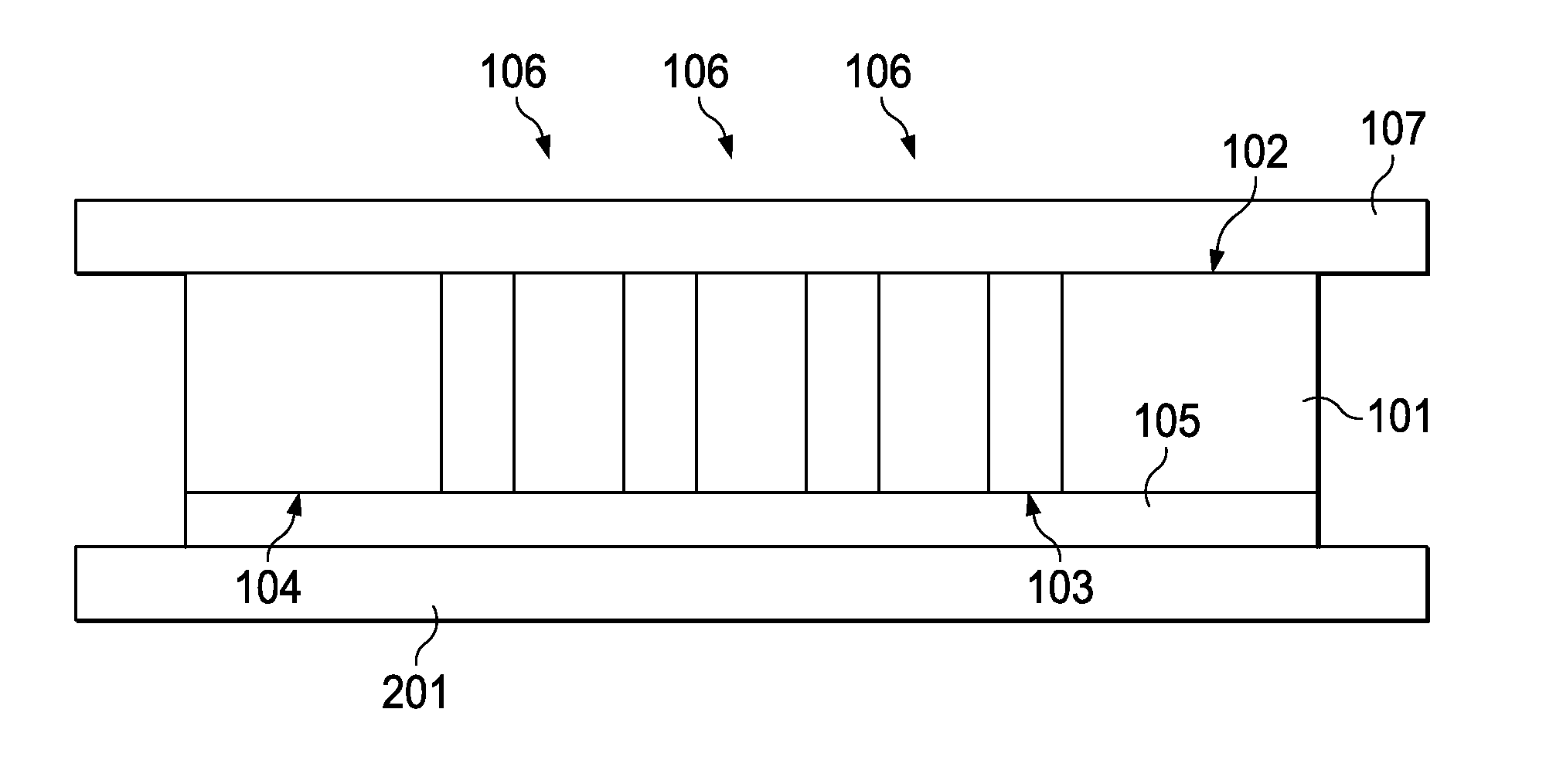
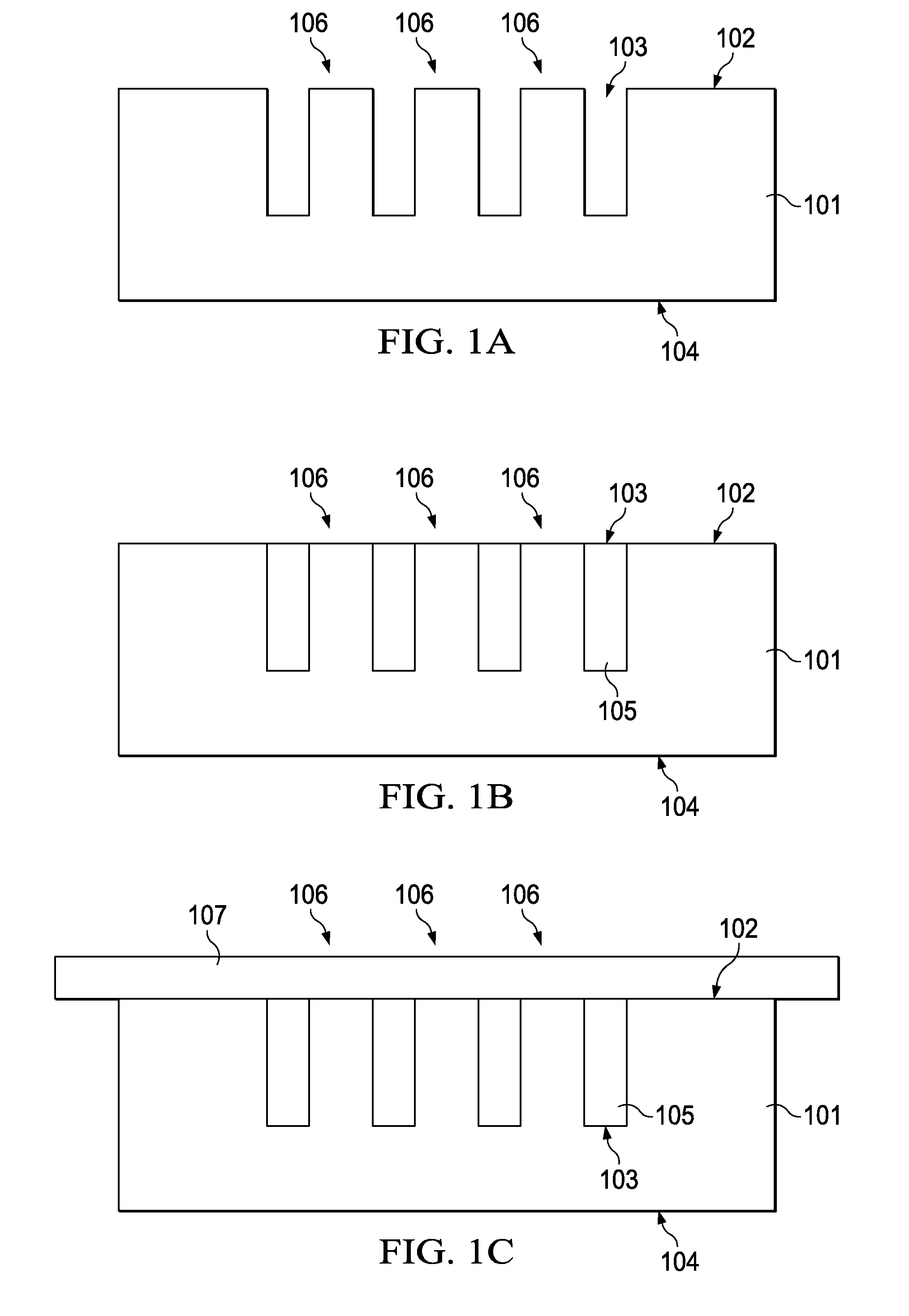
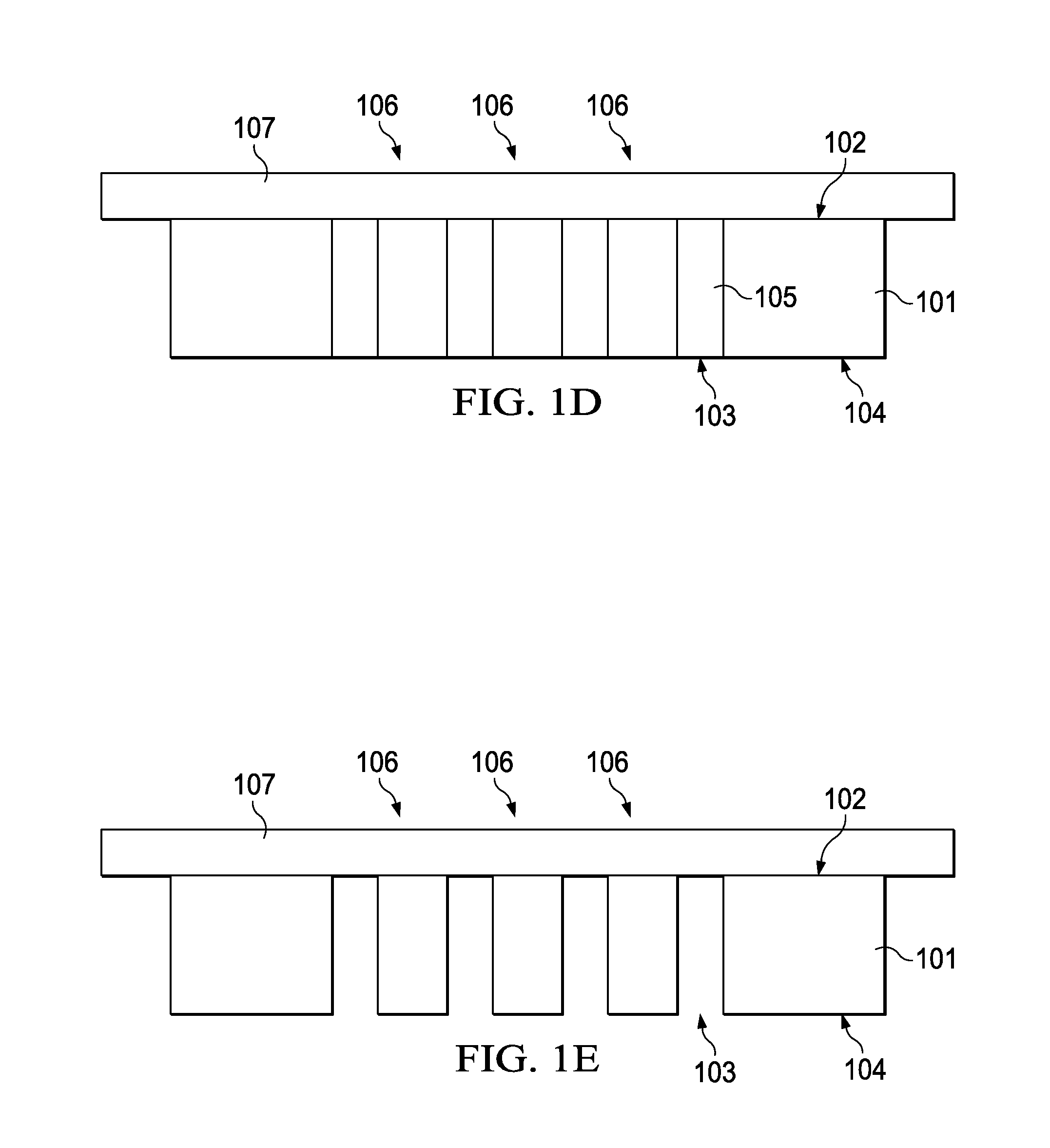
[0019]With reference now to FIG. 1A, there is shown a semiconductor wafer 101. The wafer 101 generally comprises a plurality of individual dies referred to generally by reference numeral 106, wherein each die 106 includes a substrate having electronic devices formed thereon as is known in the art. The substrate is typically co...


PUM


Abstract

A method for singulating semiconductor wafers is disclosed. A preferred embodiment comprises forming scrub lines on one side of the wafer and filling the scrub lines with a temporary fill material. The wafer is then thinned by removing material from the opposite side of the wafer from the scrub lines, thereby exposing the temporary fill material on the opposite side. The temporary fill material is then removed, and the individual die are removed from the wafer.

Description

TECHNICAL FIELD[0001]The present invention relates generally to a system and method for manufacturing semiconductor devices and, more particularly, to a system and method for separating semiconductor dies from wafers.BACKGROUND[0002]Traditionally, after multiple individual dies have been manufactured onto a single semiconductor wafer, the individual die are separated from the wafer by either cutting the wafer with a die saw or else using a nano-scrubbing process. In die sawing a large saw is used to cut the area of the wafer between adjacent dies, essentially cutting the individual die from the wafer. Unfortunately, die sawing, in addition to possible delamination and destruction of the die, also generates particles as the saw cuts through the wafer. These particles can then redeposit and contaminate the individual die, potentially causing bonding failures if the particles are larger than the bonding gap requirements (which may in some cases be less than 1 μm).[0003]A nano-scrubbing...

Claims


Application Information

Patent Timeline
Patent Type & Authority Applications(United States)
IPC IPC(8): H01L21/00
CPCH01L21/78
Inventor WU, WENG-JINYANG, KU-FENGHU, JUNG-CHIHCHIOU, WEN-CHIHYU, CHEN-HUA
Owner TAIWAN SEMICON MFG CO LTD
Why Eureka
Try Eureka