Thick oxide film for wafer backside prior to metalization loop

a metalization loop and thin oxide film technology, applied in the field of substrate processing, can solve the problems of increased rework, zero yield in portions, integrated circuits, etc., and achieve the effect of optimizing the removal of backside contamination

Active Publication Date: 2008-07-03
TEXAS INSTR INC
View PDF1 Cites 8 Cited by
  • Summary
  • Abstract
  • Description
  • Claims
  • Application Information

AI Technical Summary

Benefits of technology

[0010]According to yet another aspect of the invention, the inventor recognized that by applying a thick oxide film to the backside of the wafer, prior to the metallization loop, that the method can optimize the removal of

Problems solved by technology

Integrated circuits are particularly susceptible to contaminants both during FEOL and BEOL and therefore the wafer goes through numerous cleaning processes during the fabrication process.
Backside cross contamination, for example, can result in zero yield in portions of the wafer due to opens or shorts from pattern defocus, increased rework, decreased throughput, lower wafer yields, and the like.
Potential sources of contamination are poor maintenance of the process line, poor tool design, poor process setup, contamination from incoming wafers, contaminated handling tools, moving wafers from tool to tool, contaminants picked up in a cleaning process, and t

Method used


Image

  • Thick oxide film for wafer backside prior to metalization loop
  • Thick oxide film for wafer backside prior to metalization loop
  • Thick oxide film for wafer backside prior to metalization loop

Examples


Embodiment Construction

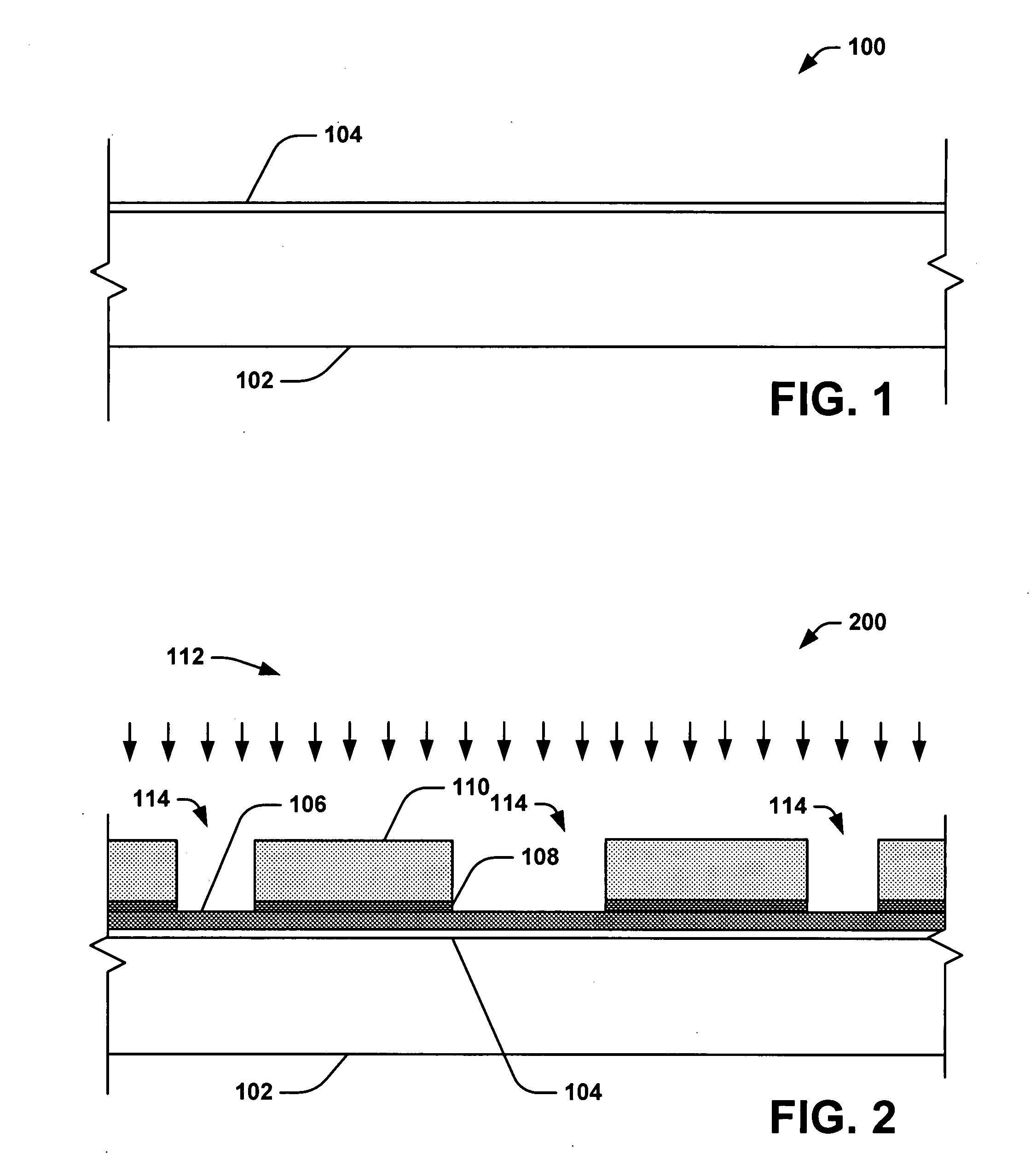
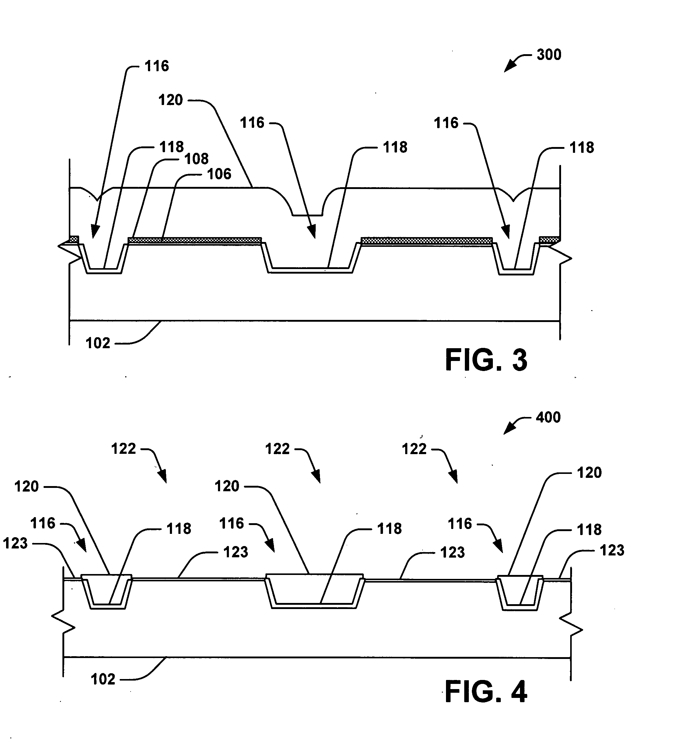
[0020]The present invention will now be described with reference to the drawings wherein like reference numerals are used to refer to like elements throughout. The present invention provides a method for depositing a thick oxide film on the backside of wafers to reduce large wafer backside contamination. However, it will be appreciated that the invention may be advantageously employed in applications other than those illustrated and described herein.

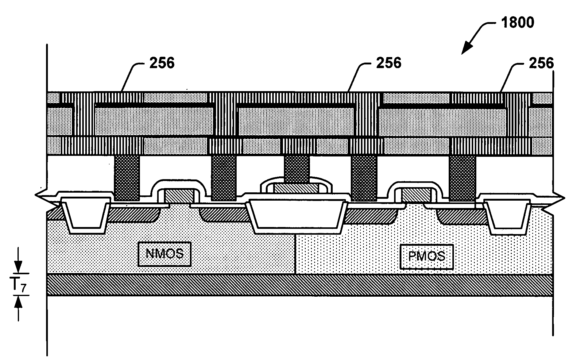
[0021]Referring to the drawings, FIGS. 1-10 are described in accordance with one embodiment of the invention that relates to front end of line processing (FEOL). FIGS. 11-18 pertain to back end of line processing (BEOL) and involves depositing a thick oxide film on a wafer backside prior to the wafer metallization loop or BEOL. The process allows semiconductor devices to be manufactured with higher yields, less processing steps, and the like. It is appreciated however that the thick oxide film could be deposited in more than one layer or...


PUM


Abstract

A method for reducing wafer backside large particle contamination, comprising: performing front end of line processing of a memory device, depositing a thick oxide on the wafer backside so that at least pre-selected oxide thickness remains after back end of line processing is complete and performing the back end of line processing of the memory device.

Description

REFERENCE TO RELATED APPLICATIONS[0001]This application claims priority to Ser. No. 60 / 877,782 filed Dec. 29, 2006, which I entitled “Thick Oxide Film for Wafer Backside Prior to Metalization Loop”.FIELD OF THE INVENTION[0002]The present invention relates generally to substrate processing and more particularly to an improved method for reducing wafer backside large particle contamination.BACKGROUND OF THE INVENTION[0003]Integrated circuit (IC) fabrication on a silicon wafer can be thought of as “front end of the line” processing (FEOL) and “back end of the line” processing (BEOL). FEOL processing is frequently the fabrication of various devices on the topside layer of the wafer and BEOL is normally perceived as electrically interconnecting the various devices created in the FEOL processing. Integrated circuits are particularly susceptible to contaminants both during FEOL and BEOL and therefore the wafer goes through numerous cleaning processes during the fabrication process. The con...

Claims


Application Information

Patent Timeline
IPC IPC(8): H01L21/31H01L21/768
CPCH01L21/02065H01L21/02074H01L21/02164H01L21/02271H01L21/28518H01L21/3081H01L27/1052H01L21/3162H01L21/76808H01L21/76829H01L21/8238H01L21/823892H01L21/31612H10B99/00
Inventor ANDERSON, NHAN HANH
Owner TEXAS INSTR INC
Why Eureka
Try Eureka