Ceramic sprayed member, making method, abrasive medium for use therewith

a technology of ceramic sprayed coating and making method, which is applied in the direction of manufacturing tools, mechanical vibration separation, energy-based chemical/physical/physico-chemical processes, etc., can solve the problems of surface contamination and yttrium contamination of wafers, and achieve stable manufacture and improved plasma resistance. , the effect of reducing the contamination of the surfa

Inactive Publication Date: 2013-05-16
SHIN ETSU CHEM CO LTD
View PDF6 Cites 6 Cited by
  • Summary
  • Abstract
  • Description
  • Claims
  • Application Information

AI Technical Summary

Benefits of technology

[0013]Moreover, to achieve a further reduction of production cost of the semiconductor fabrication process, the initial run using dummy wafers is required to reduce the running time and the number of wafers.
[0014]An object of the invention is to provide ceramic sprayed members with improved plasma resistance, which cause only a minimal level of contamination to wafers and ensure stable manufacture when used in a halogen plasma process for semiconductor fabrication or the like; a method for preparing the same; and an abrasive medium for use with ceramic sprayed members.
[0015]Making efforts for the purpose of mitigating wafer contamination, the inventors have found that use of a halogen plasma corrosion resistant member having a sprayed coating from which a potential particulate contamination source has been removed, that is, a sprayed coating from which splats on its surface have been removed is effective in reducing an amount of initially released particles.
[0022]The ceramic sprayed member with improved plasma resistance mitigates particle contamination of wafers and enables stable manufacture when used in a halogen plasma process for semiconductor fabrication or the like.

Problems solved by technology

Although the yttrium oxide sprayed members are successful in reducing contamination with newborn particles of aluminum fluoride or the like, another problem becomes highlighted that wafers are contaminated with yttrium.
The blast of alumina alone, however, suffers from such problems as excessive abrasion of members, difficult thickness control due to excessive abrasion, and retention of blasted grains sticking into the surface, which causes surface contamination again.

Method used


Image

  • Ceramic sprayed member, making method, abrasive medium for use therewith
  • Ceramic sprayed member, making method, abrasive medium for use therewith
  • Ceramic sprayed member, making method, abrasive medium for use therewith

Examples


example 1

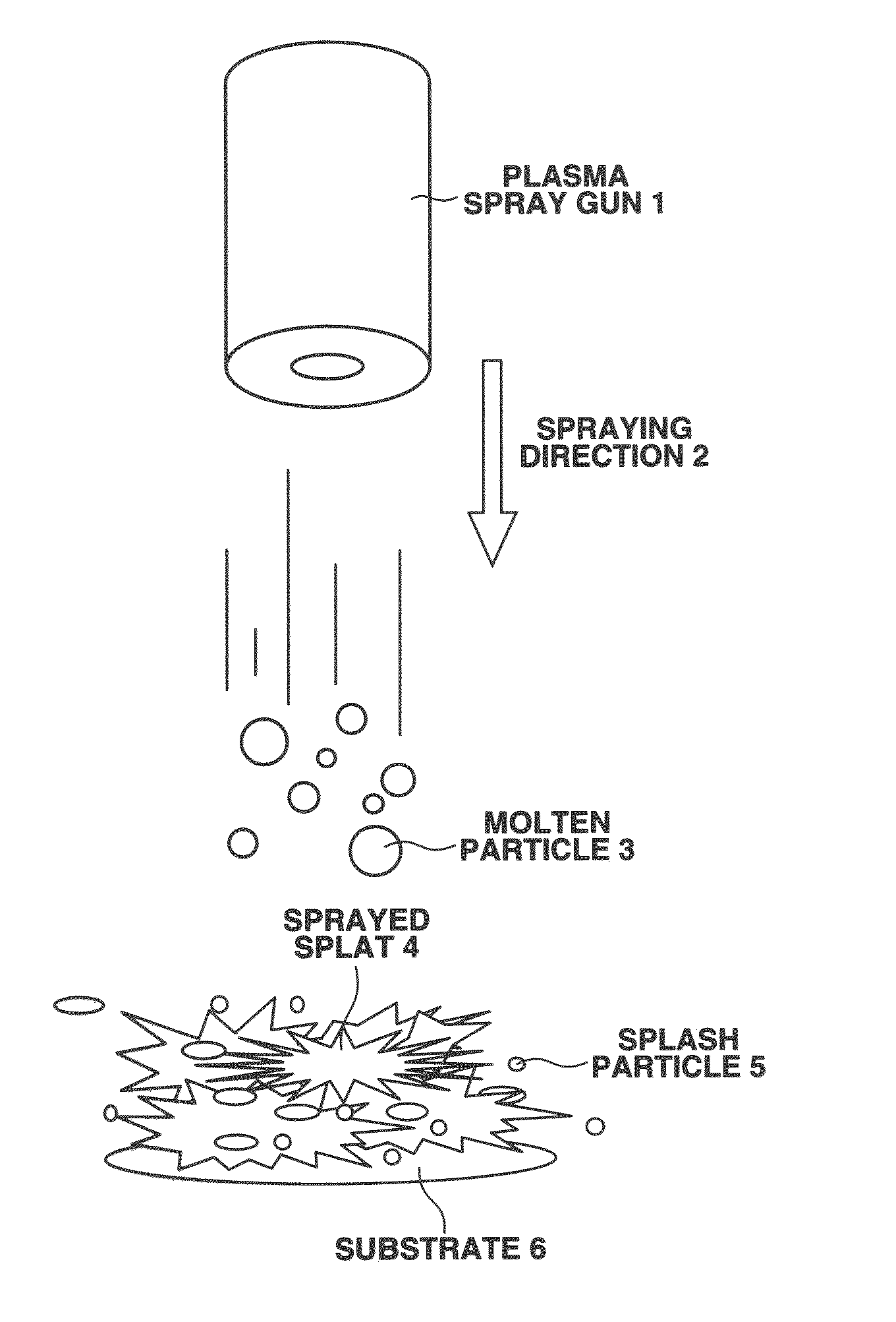
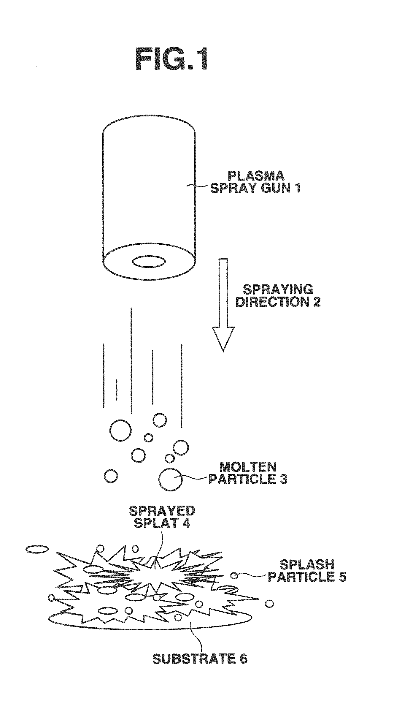
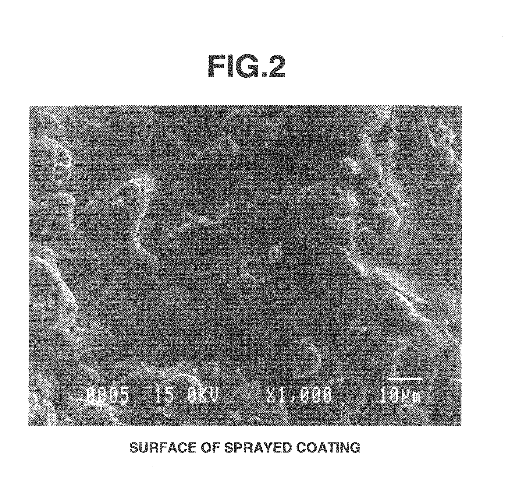
[0042]A surface of an aluminum alloy substrate of 100 mm square was degreased with acetone and roughened with corundum abrasive. Yttrium oxide powder was sprayed onto the roughened surface by means of an atmospheric plasma spray apparatus, using argon gas as the plasma gas, a power of 40 kW, a spray distance of 100 mm, and a deposition rate of 30 μm / pass. A yttrium oxide coating of 250 μm thick was deposited.

[0043]The surface of the sprayed coating was then abraded by blasting an elastomeric medium containing 50% by volume of #1500 SiC (GC) abrasive grains in ethylene-propylene-diene rubber (EPDM) having an average particle size of about 500 μm for 10 minutes. A sample having a coating of 220 μm thick was obtained.

[0044]The sample was measured for surface roughness by an instrument Handysurf E-35A (Tokyo Seimitsu Co., Ltd.), with the data plotted as a surface roughness curve in FIG. 7.

example 2

[0045]A surface of an aluminum alloy substrate of 100 mm square was degreased with acetone and roughened with corundum abrasive. Yttrium fluoride powder was sprayed onto the roughened surface by means of an atmospheric plasma spray apparatus, using argon gas as the plasma gas, a power of 40 kW, a spray distance of 100 mm, and a deposition rate of 30 μm / pass. A yttrium fluoride coating of 250 μm thick was deposited.

[0046]The surface of the sprayed coating was blasted with the same elastomeric medium as in Example 1 for 10 minutes. A sample having a coating of 220 gm thick was obtained.

example 3

[0047]A surface of an aluminum alloy disc having a diameter of 400 mm (serving as a ring-shaped semiconductor etcher member) was degreased with acetone and roughened with corundum abrasive. Yttrium oxide powder was sprayed onto the roughened surface by means of an atmospheric plasma spray apparatus, using argon gas as the plasma gas, a power of 40 kW, a spray distance of 100 mm, and a deposition rate of 30 μm / pass. A yttrium oxide coating of 250 μm thick was deposited.

[0048]The surface of the sprayed coating was blasted with the same elastomeric medium as in Example 1 for 30 minutes.

[0049]A member having a coating of 220 μm thick was obtained.


PUM

PropertyMeasurementUnit
particle sizeaaaaaaaaaa
thicknessaaaaaaaaaa
thicknessaaaaaaaaaa

Abstract

A ceramic sprayed member comprises a substrate and a ceramic sprayed coating thereon. Splats have been removed from the surface of the sprayed coating, typically by blasting. The ceramic sprayed member with improved plasma resistance mitigates particle contamination of wafers and enables stable manufacture when used in a halogen plasma process for semiconductor fabrication or the like.

Description

CROSS-REFERENCE TO RELATED APPLICATION[0001]This application is a divisional application of U.S. patent application No. 12 / 359,116, filed Jan. 23, 2009, and claims priority under 35 U.S.C. §119(a) of Japanese Patent Application No. 2008-013620, filed Jan. 24, 2008, the entire contents of which are hereby incorporated by reference.TECHNICAL FIELD[0002]This invention relates to surface tailoring of ceramic sprayed coatings, and more particularly, to ceramic sprayed members for use as plasma-resistant members in plasma processing apparatus, typically dry etching apparatus in the semiconductor and flat panel display fabrication industries, and a method for preparing the same. It also relates to abrasive media for use with ceramic sprayed members.BACKGROUND ART[0003]As is well known in the art, systems for the fabrication of semiconductor devices and flat panel displays such as liquid crystal displays and organic or inorganic electroluminescent displays often operate in a halogen-based c...

Claims


Application Information

Patent Timeline
Patent Type & Authority Applications(United States)
IPC IPC(8): B05D3/02B05D3/12
CPCC23C4/10C23C4/105H01L21/67069C23C4/18H01J37/32477C23C4/127C23C4/11C23C4/134B24D3/10H01L21/68
Inventor MAEDA, TAKAONAKANO, HAJIMETSUKATANI, TOSHIHIKO
Owner SHIN ETSU CHEM CO LTD
Why Eureka
Try Eureka