Electronic devices including carbon-based films having sidewall liners, and methods of forming such devices

a technology of sidewall liners and electrodes, which is applied in the direction of bulk negative resistance effect devices, semiconductor devices, electrical equipment, etc., can solve the problems of low resistance, difficult to fill gaps with high-aspect ratio, and difficult to reduce the resistance of the devi

Active Publication Date: 2010-01-21
SANDISK TECH LLC
View PDF23 Cites 63 Cited by
  • Summary
  • Abstract
  • Description
  • Claims
  • Application Information

AI Technical Summary

Problems solved by technology

The substrates may be thinned or removed from the memory levels before bonding, but as the memory levels are initially formed over separate substrates, such memories are not true monolithic three dimensional memory arrays.
Application of a programming voltage permanently changes the nature of the polysilicon, rendering it low-resistance.
Very high-aspect ratio gaps are difficult to fill without voids.

Method used


Image

  • Electronic devices including carbon-based films having sidewall liners, and methods of forming such devices
  • Electronic devices including carbon-based films having sidewall liners, and methods of forming such devices
  • Electronic devices including carbon-based films having sidewall liners, and methods of forming such devices

Examples


Embodiment Construction

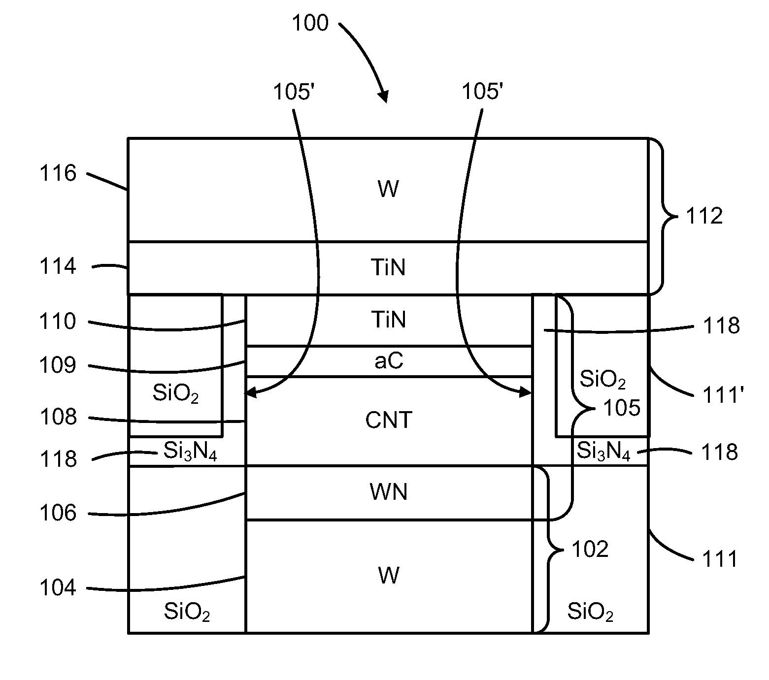
[0012]Certain carbon-based films, including but not limited to carbon nanotubes (“CNTs”), graphene, amorphous carbon containing microcrystalline or other regions of graphene, and other graphitic carbon films, etc., may exhibit resistivity switching properties that may be used to form microelectronic non-volatile memories. Such films therefore are candidates for integration within a three-dimensional memory array. For instance, CNT materials have demonstrated memory switching properties on lab-scale devices with a 100× separation between ON and OFF states and mid-to-high range resistance changes. Such a separation between ON and OFF states renders CNT materials viable candidates for memory cells formed using the CNT materials in series with vertical diodes, thin film transistors or other steering elements.

[0013]In the aforementioned example, a metal-insulator-metal (“MIM”) stack formed from a carbon-based material sandwiched between two metal or otherwise conducting layers may serve ...


PUM


Abstract

Methods in accordance with aspects of this invention form microelectronic structures in accordance with other aspects of this invention, such as non-volatile memories, that include (1) a layerstack having a pattern including sidewalls, the layerstack comprising a resistivity-switchable layer disposed above and in contact with a bottom electrode, and a top electrode disposed above and in contact with the resistivity-switchable layer; and (2) a dielectric sidewall liner in contact with the sidewalls of the layerstack; wherein the resistivity-switchable layer includes a carbon-based material, and the dielectric sidewall liner includes an oxygen-poor dielectric material. Numerous additional aspects are provided.

Description

CROSS-REFERENCE TO RELATED APPLICATIONS[0001]This application claims the benefit of U.S. Patent Application Ser. No. 61 / 081,029, filed 15 Jul. 2008, “METHODS FOR ETCHING CARBON NANO-TUBE FILMS” (the '029 application), which is incorporated by reference herein in its entirety for all purposes. (Docket No. MXA-315P).FIELD OF THE INVENTION[0002]This invention relates to microelectronic devices, such as non-volatile memories, and more particularly to electronic devices including carbon-based films having sidewall liners, and methods of forming the same.BACKGROUND[0003]Non-volatile memories formed from reversible resistance-switching elements are known. For example, U.S. patent application Ser. No. 11 / 968,154, filed Dec. 31, 2007, titled “MEMORY CELL THAT EMPLOYS A SELECTIVELY FABRICATED CARBON NANO-TUBE REVERSIBLE RESISTANCE-SWITCHING ELEMENT AND METHODS OF FORMING THE SAME” (hereinafter “the '154 Application”), which is hereby incorporated by reference herein in its entirety for all pu...

Claims


Application Information

Patent Timeline
Patent Type & Authority Applications(United States)
IPC IPC(8): H01L45/00H01L21/30
CPCH01L27/101H01L45/04H01L45/1233H01L27/2481H01L45/1675H01L27/2409H01L45/149H10B63/20H10B63/84H10N70/20H10N70/826H10N70/8845H10N70/063
Inventor SCHRICKER, APRIL D.
Owner SANDISK TECH LLC
Why Eureka
Try Eureka