Structure and Method for Forming Trench Gate Transistors with Low Gate Resistance

a transistor and trench gate technology, applied in the field of semiconductor technology, can solve the problems of limited success of the gate resistance reduction techniques proposed to da

Inactive Publication Date: 2010-01-21
SEMICON COMPONENTS IND LLC
View PDF98 Cites 33 Cited by
  • Summary
  • Abstract
  • Description
  • Claims
  • Application Information

AI Technical Summary

Benefits of technology

[0005]In accordance with an embodiment of the invention, a field effect transistor includes body regions of a first conductivity type over a semiconductor region of a second conductivity type such that the body regions form p-n junctions with the semiconductor region. Trenches extend through the body region and terminate within the semiconductor region. Source regions of the second conductivity type extend over the body regions adjacent the trenches such that the source regions form p-n junctions with the body regions. A gate dielectric layer lines sidewalls of each trench. A metal liner lines the gate dielectric layer in each trench. A gate electrode comprising metallic material is disposed in each trench.

Problems solved by technology

However, techniques proposed to date for reducing the gate resistance have had limited success.

Method used


Image

  • Structure and Method for Forming Trench Gate Transistors with Low Gate Resistance
  • Structure and Method for Forming Trench Gate Transistors with Low Gate Resistance
  • Structure and Method for Forming Trench Gate Transistors with Low Gate Resistance

Examples


Embodiment Construction

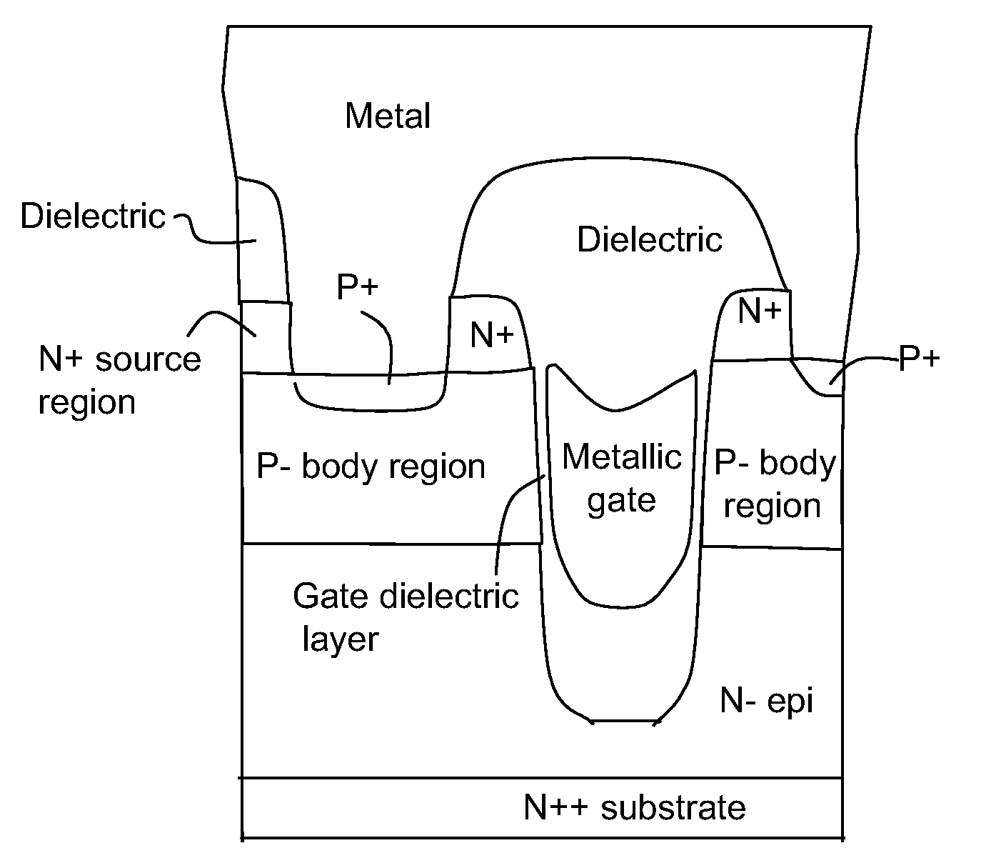
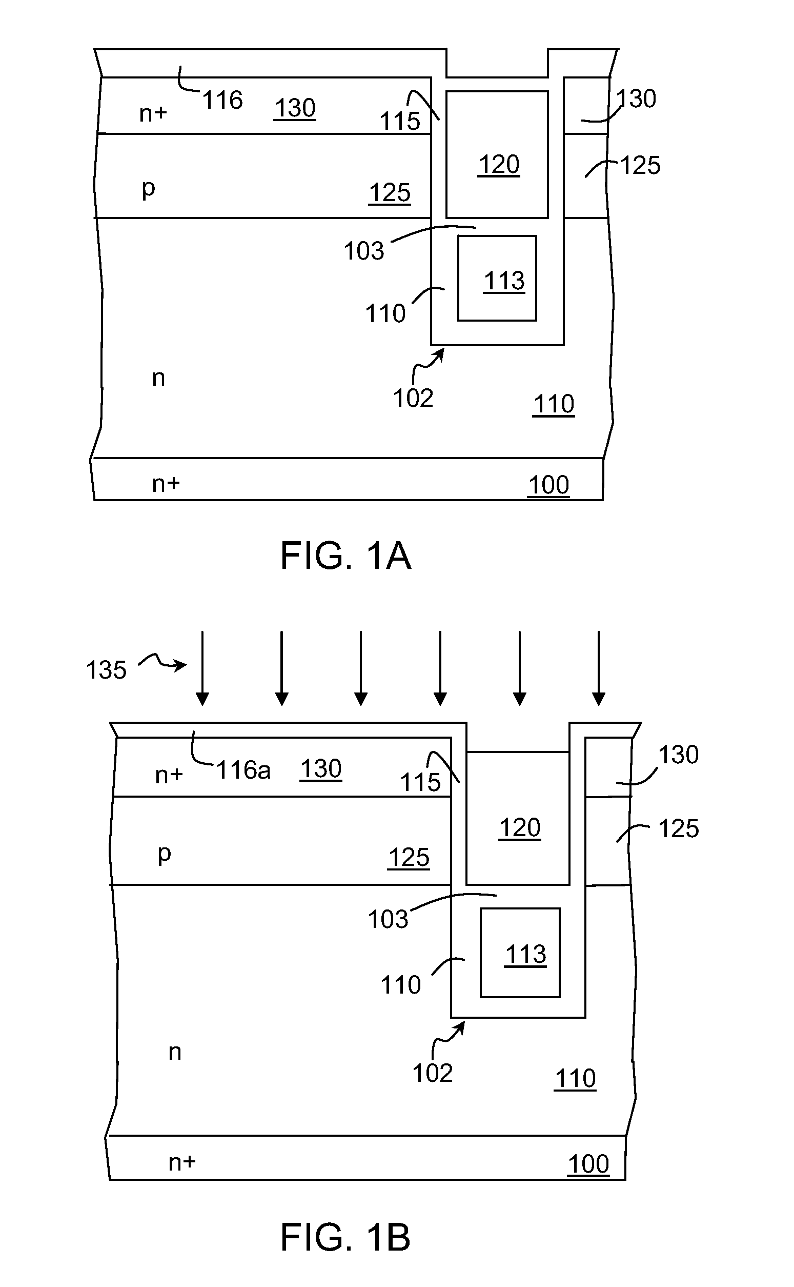
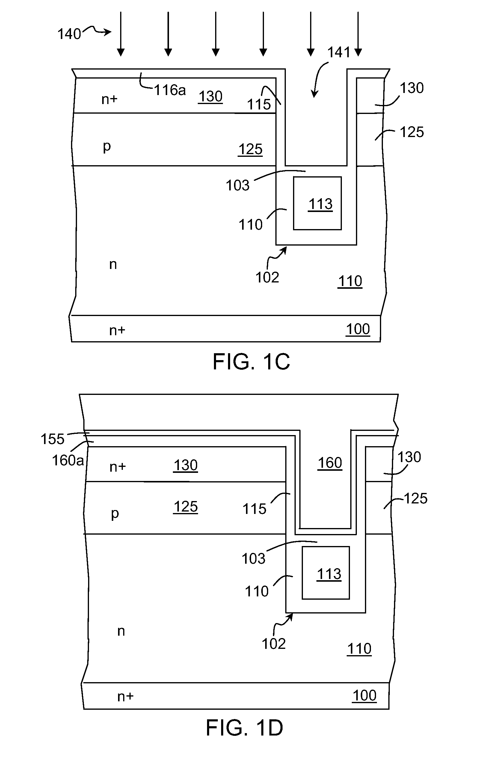
[0022]In accordance with embodiments of the present invention, techniques directed to integrated circuits and their processing are described. More particularly, in some embodiments, power field effect transistors (FETs) include metallic gate electrodes to advantageously substantially reduce the gate resistance compared to conventional polysilicon gates. A simple process technique is disclosed whereby a polysilicon gate electrode formed in trenches in accordance with conventional techniques is removed and replaced with a metallic gate electrode without using any masking steps. The simple process sequence for removal and replacement of poly gates with metallic gates can easily be integrated with existing processes for forming power MOSFETs without requiring additional masking steps. Merely by way of example, the techniques according to the invention have been applied to trench power MOSFETs, but the invention has a much broader range of applicability. For example, the techniques accor...


PUM


Abstract

A field effect transistor includes body regions of a first conductivity type over a semiconductor region of a second conductivity type such that the body regions form p-n junctions with the semiconductor region. Trenches extend through the body region and terminate within the semiconductor region. Source regions of the second conductivity type extend over the body regions adjacent the trenches such that the source regions form p-n junctions with the body regions. A gate dielectric layer lines sidewalls of each trench. A metal liner lines the gate dielectric layer in each trench. A gate electrode comprising metallic material is disposed in each trench.

Description

CROSS-REFERENCES TO RELATED APPLICATIONS[0001]This application claims the benefit of U.S. Provisional Application No. 61 / 013,985, filed Dec. 14, 2007, which is incorporated herein by reference in its entirety for all purposes.BACKGROUND OF THE INVENTION[0002]The present invention relates in general to semiconductor technology and more particularly to trench gate field effect transistors (FETs) with low gate resistance and methods for forming the same.[0003]Generally, an n-channel trench-gate power MOSFET includes an n-type substrate on which an n-type epitaxial layer is formed. The substrate embodies the drain of the MOSFET. A p-type body region extends into the epitaxial layer. Trenches extend through the body region and into the portion of the epitaxial layer bounded by the body region and the substrate (commonly referred to as the drift region). A gate dielectric layer is formed on the sidewalls and bottom of each trench. Source regions flank the trenches. Heavy body regions are ...

Claims


Application Information

Patent Timeline
Patent Type & Authority Applications(United States)
IPC IPC(8): H01L29/78H01L21/336
CPCH01L29/407H01L29/41766H01L29/42368H01L29/456H01L29/7397H01L29/4966H01L29/66727H01L29/66734H01L29/4958
Inventor PAN, JAMES
Owner SEMICON COMPONENTS IND LLC
Why Eureka
Try Eureka