Organic light emitting display device

a light-emitting display and organic technology, applied in semiconductor devices, instruments, computing, etc., can solve problems such as degrading the luminance of emitted light, and achieve the effect of improving luminance without increasing the thickness of the touch panel

Active Publication Date: 2010-01-21
SAMSUNG DISPLAY CO LTD
View PDF57 Cites 154 Cited by
  • Summary
  • Abstract
  • Description
  • Claims
  • Application Information

AI Technical Summary

Benefits of technology

[0008]Embodiments of the present invention provide an organic light emitting display device including an encapsulation substrate, an inner surface of which is patterned using an indium tin oxide (ITO) pattern and openings are f

Problems solved by technology

Another problem is that indium tin oxide (ITO) electrodes are disposed on the entire surface of an encapsulation substrate to provide the touch panel functio

Method used


Image

  • Organic light emitting display device
  • Organic light emitting display device
  • Organic light emitting display device

Examples


first embodiment

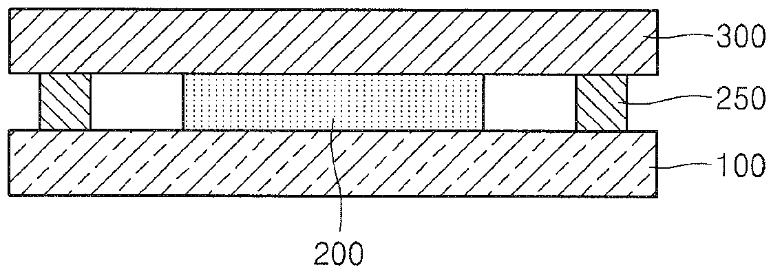
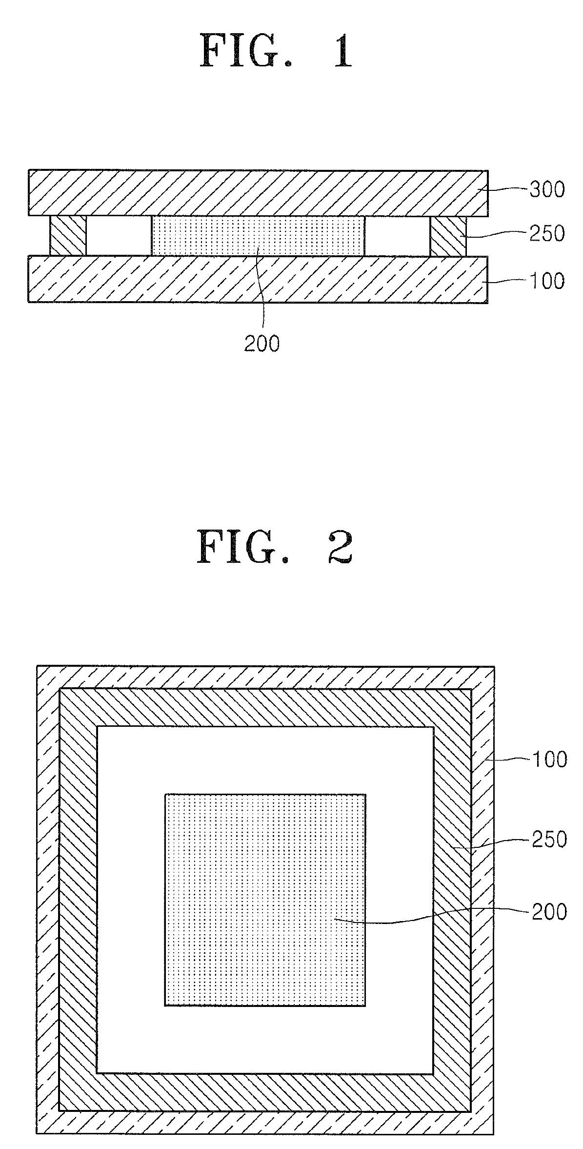
[0050]FIG. 1 is a schematic drawing illustrating a cross-sectional view of a portion of an organic light emitting display device according to a first embodiment of the present invention, and FIG. 2 is a schematic drawing illustrating a plan view of the organic light emitting display device of FIG. 1. In FIG. 2, an encapsulation substrate 300 illustrated in FIG. 1 is not shown.

[0051]Referring to FIGS. 1 and 2, a display unit 200 including a plurality of organic light emitting diodes (OLEDs) is formed on a substrate 100.

[0052]The substrate 100 is, for example, formed of a transparent glass containing SiO2 as a main component, but the present invention is not limited thereto, and thus the substrate 100 may also be formed of a transparent plastic material that may be an insulating organic material selected from the group consisting of polyethersulphone (PES), polyacrylate (PAR), polyetherimide (PEI), polyethyelene napthalate (PEN), polyethyelene terephthalate (PET), polyphenylene sulfid...

second embodiment

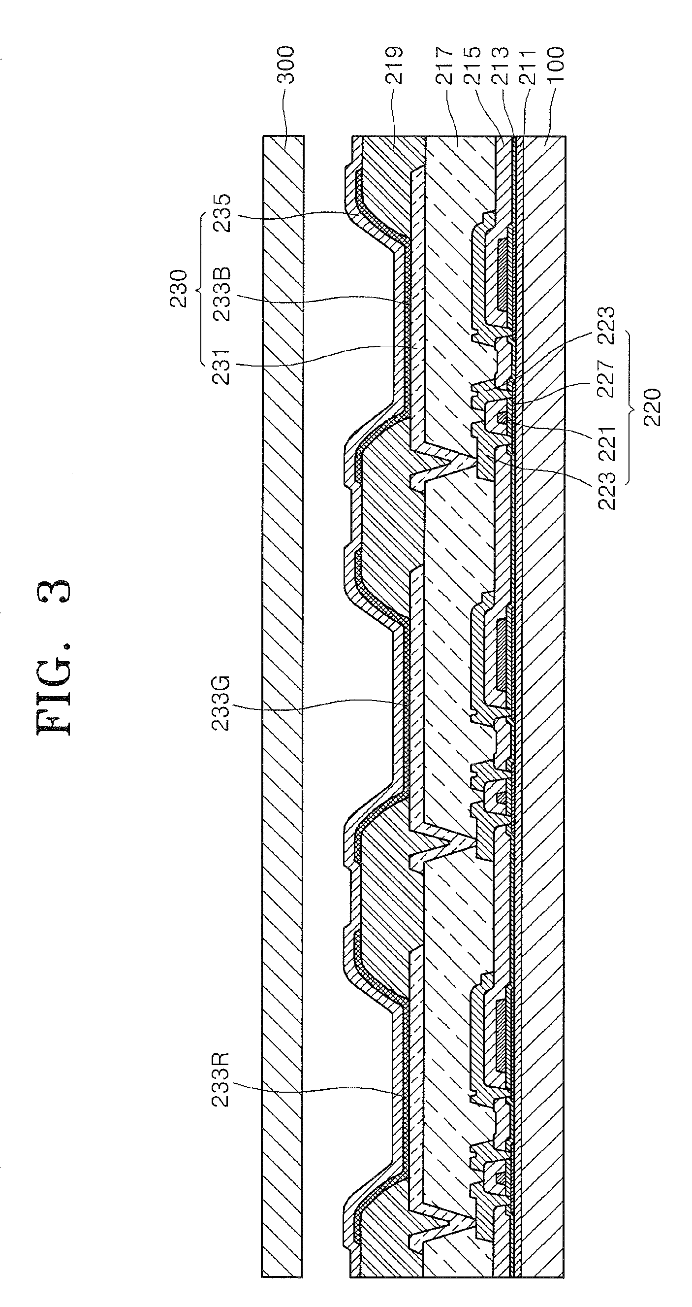
[0101]FIG. 8A is a schematic drawing illustrating a bottom view of an encapsulation substrate with a first pattern layer formed on a surface of the encapsulation substrate in an organic light emitting display device according to a second embodiment of the present invention. FIG. 8B is a schematic drawing illustrating a bottom view of the first pattern layer of FIG. 8A and a second pattern layer on the first pattern layer. FIG. 8C is a schematic drawing illustrating a cross-sectional view taken along a line VIII-VIII in FIG. 8B. FIG. 8D is a schematic drawing illustrating a perspective view of the first pattern layer and the second pattern layer of FIG. 8B.

[0102]Referring to FIGS. 8A through 8D, a first pattern layer 410, a first insulating layer 430, a second pattern layer 420, and a second insulating layer 440 are respectively formed on a surface of an encapsulation substrate 400 so as to face a substrate.

[0103]Different from the first embodiment, the second embodiment shown in FIG...


PUM


Abstract

An organic light emitting display device having an electrostatic capacitive type touch panel function with reduced thickness and improved luminance. A display panel of the organic light emitting display device includes a substrate, a display unit having a plurality of pixels on the substrate, and a touch sensing unit on the display unit. The touch sensing unit includes an encapsulation substrate and a capacitive pattern layer on a side of the encapsulation substrate facing the display unit. The capacitive pattern layer has a plurality of openings corresponding in position to the plurality of pixels.

Description

CROSS-REFERENCE TO RELATED APPLICATIONS[0001]This application claims priority to and the benefit of U.S. Provisional Patent Application No. 61 / 082,424, filed on Jul. 21, 2008, the entire content of which is incorporated herein by reference. This application is related to U.S. patent application Ser. No. 12 / 350,101 filed on Jan. 7, 2009, the entire content of which is incorporated herein by reference.BACKGROUND OF THE INVENTION[0002]1. Field of the Invention[0003]The present invention relates to an organic light emitting display device, and more particularly, to an organic light emitting display device having a touch panel function.[0004]2. Description of the Related Art[0005]Among various kinds of flat display devices, an organic light emitting display device is an active matrix type display device with a wide viewing angle, high contrast, and fast response speed. In comparison to an inorganic light emitting display device, the organic light emitting display device having an emissiv...

Claims


Application Information

Patent Timeline
IPC IPC(8): G09G3/30
CPCG06F3/0412H01L27/323G06F2203/04111G06F3/044G06F3/0443H10K59/40G06F2203/04103G06F3/0446H10K59/12H10K2102/103H10K2102/311H10K2102/341
Inventor KIMCHOI, JONG-HYUNIM, CHOONG-YOULLEE, IL-JEONG
Owner SAMSUNG DISPLAY CO LTD
Why Eureka
Try Eureka