

Method of fabricating strained silicon transistor
- Summary
- Abstract
- Description
- Claims
- Application Information
AI Technical Summary
Benefits of technology
Problems solved by technology
Method used
Image

Examples
first embodiment
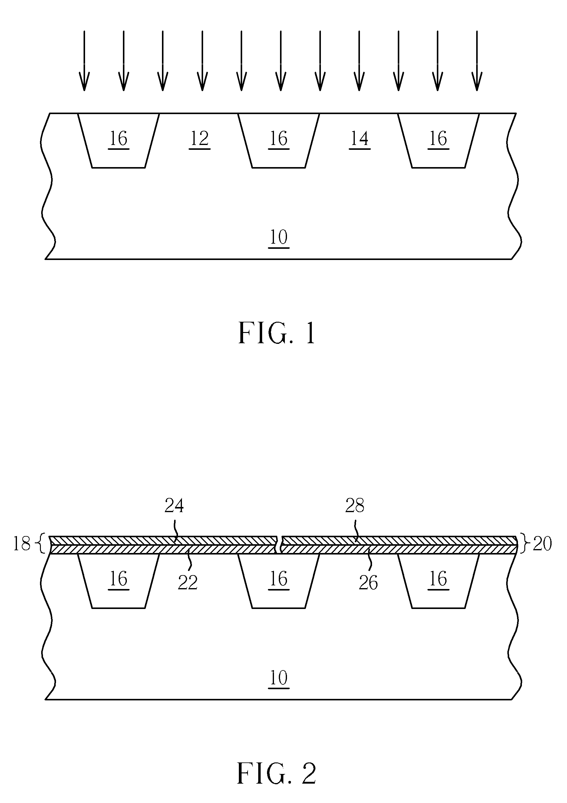
[0029]As shown in FIG. 6, first a substrate 10 is provided. There is a first transistor region 12 and a second transistor region 14 on the substrate 10. Secondly, an insulator such as a shallow trench isolation (STI) 16 is formed in the substrate 10 to segregate the first transistor region 12 and the second transistor region 14. The procedures of fabricating the shallow trench isolation (STI) 16 have already been illustrated in the first embodiment and therefore the details are not described here. The first transistor region 12 is used to form the active area of a transistor of a first conductivity type. In other words, the transistor in the first transistor region 12 is of a first conductivity type, such as an N-type MOS. The second transistor region 14 is used to form the active area of a transistor of a second conductivity type. In other words, the transistor in the second transistor region 14 is of a second conductivity type, such as a P-type MOS.
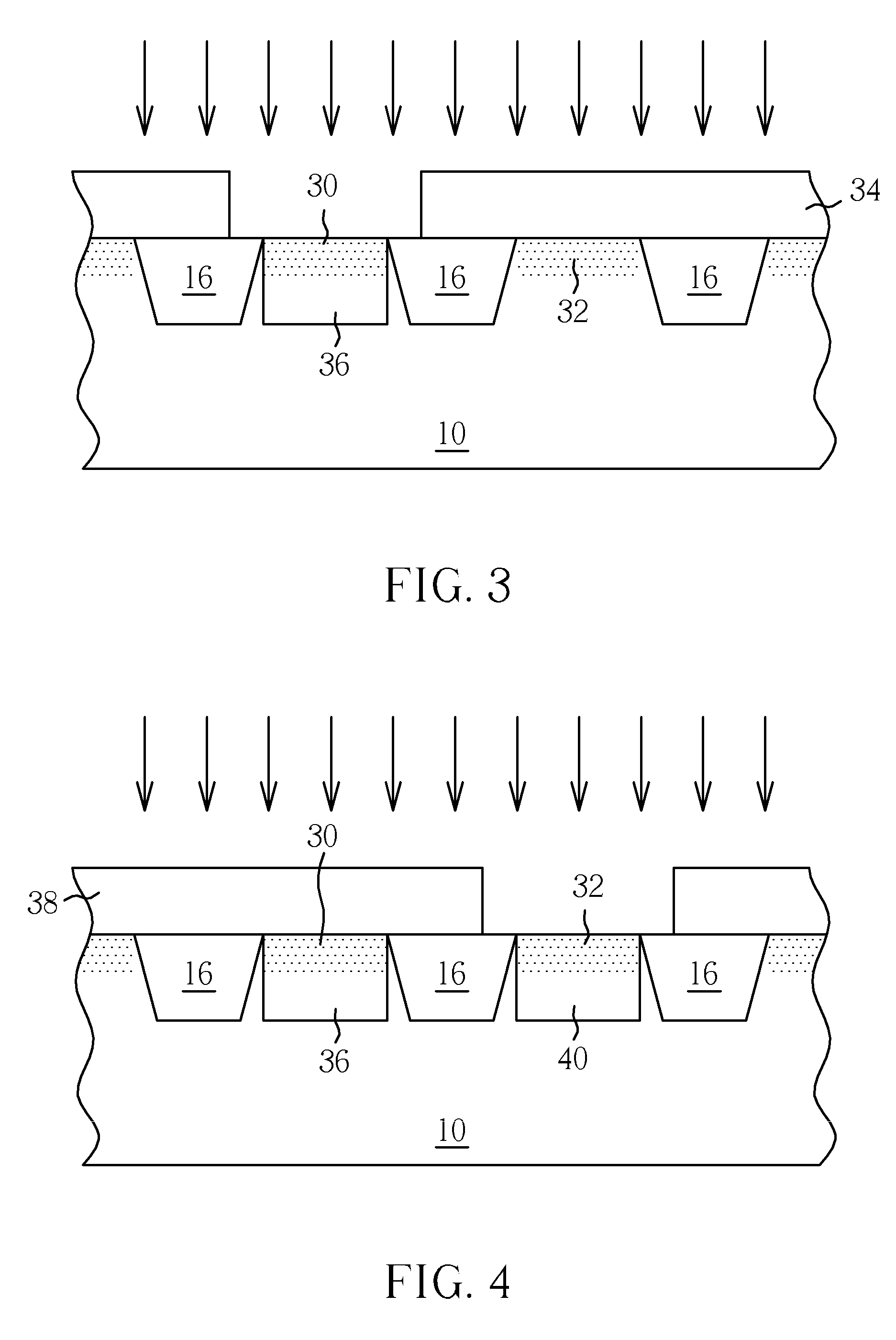
[0030]To be continued, a pattern...
second embodiment
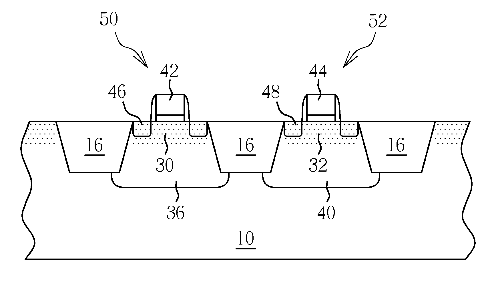
[0038]Additionally, the advantages of the present invention reside in that the same patterned photoresist is used for both the first amorphous silicon procedure and the first high-concentration ion implantation procedure, and another same patterned photoresist is used for both the second amorphous silicon procedure and the second high-concentration ion implantation procedure. Moreover, the same annealing procedure is used for driving and for activating the dopants in the doped well, for the first strained layer and for the second strained layer, and may be performed in the same chamber without switching between different vacuum chambers. Furthermore, as shown in FIG. 10b, if the operational order of the amorphous silicon procedure and the doped well ion implantation procedure is exchanged, this can result in another method for the strained silicon transistor of the present invention.
[0039]Please refer to FIGS. 11-13, which illustrate a fourth preferred embodiment for fabricating a t...
fifth embodiment
[0053]Additionally, the advantages of the present invention resides in that the same patterned photoresist is used for both the amorphous silicon procedure and the high-concentration ion implantation procedure. Moreover, the same annealing procedure is used for driving and for activating the dopants in the doped well and for the strained layer, and may be performed in the same chamber without switching between different vacuum chambers. Furthermore, as shown in FIG. 17b, if the operational order of the amorphous silicon procedure and the doped well ion implantation procedure is exchanged, it can result in still another method for the strained silicon transistor of the present invention.
[0054]Those skilled in the art will readily observe that numerous modifications and alterations of the device and method may be made while retaining the teachings of the invention.
PUM
 Abstract
Description
Claims
Application Information