Implementing Reduced Hot-Spot Thermal Effects for SOI Circuits

a technology of silicononinsulator and hot spot thermal effect, which is applied in the direction of semiconductor devices, semiconductor device details, electrical apparatus, etc., can solve the problems of inability to keep the device junction temperature under the reliability and/or function limitations, severe performance requirements, and power dissipation of chips such as processors, controllers, etc., and achieve the effect of reducing hot spot thermal effects and reducing hotspot thermal effects

Inactive Publication Date: 2010-01-28
IBM CORP
View PDF6 Cites 49 Cited by
  • Summary
  • Abstract
  • Description
  • Claims
  • Application Information

AI Technical Summary

Benefits of technology

[0010]Principal aspects of the present invention are to provide methods and structures for implementing reduced hot spot thermal effects for silicon-on-insulator (SOI) circuits. Other important aspects of the present invention are to

Problems solved by technology

Typical semiconductor applications today have reached the point where the ability to keep the device junction temperatures under the limitations established for reliability and/or function and performance requirements are severely limited.
These issues are exasperated

Method used


Image

  • Implementing Reduced Hot-Spot Thermal Effects for SOI Circuits
  • Implementing Reduced Hot-Spot Thermal Effects for SOI Circuits
  • Implementing Reduced Hot-Spot Thermal Effects for SOI Circuits

Examples


Embodiment Construction

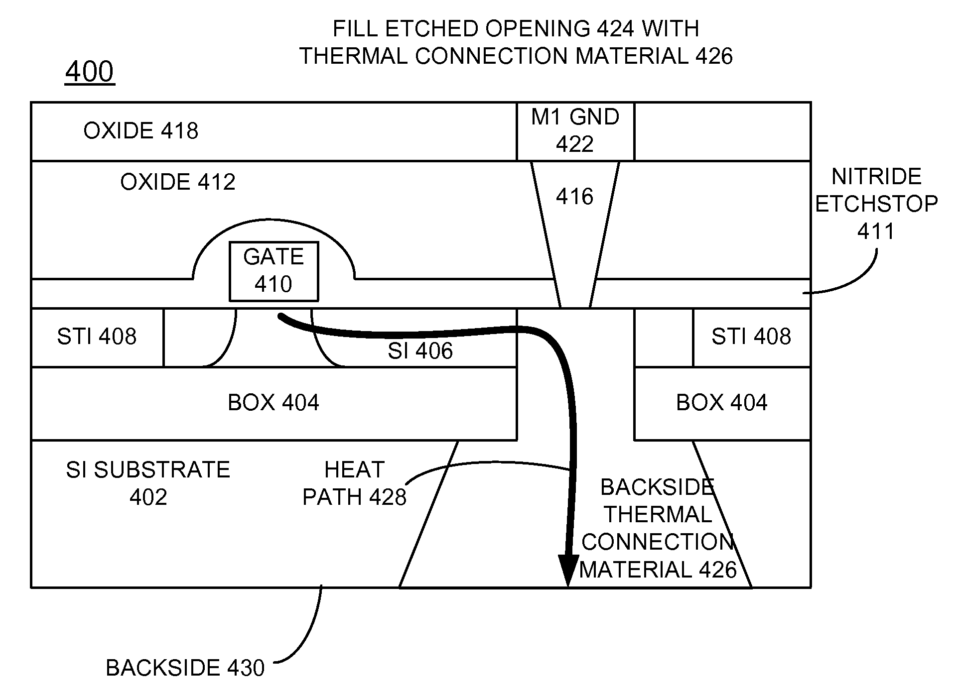
[0021]In accordance with features of one embodiment of the invention, methods and structures are provided for implementing reduced hot spot thermal effects for silicon-on-insulator (SOI) circuits. A thermal conductive path is built to reduce thermal effects of a hotspot area for SOI circuits. The thermal conductive path of the invention extends from the active layer to the backside of the SOI structure.

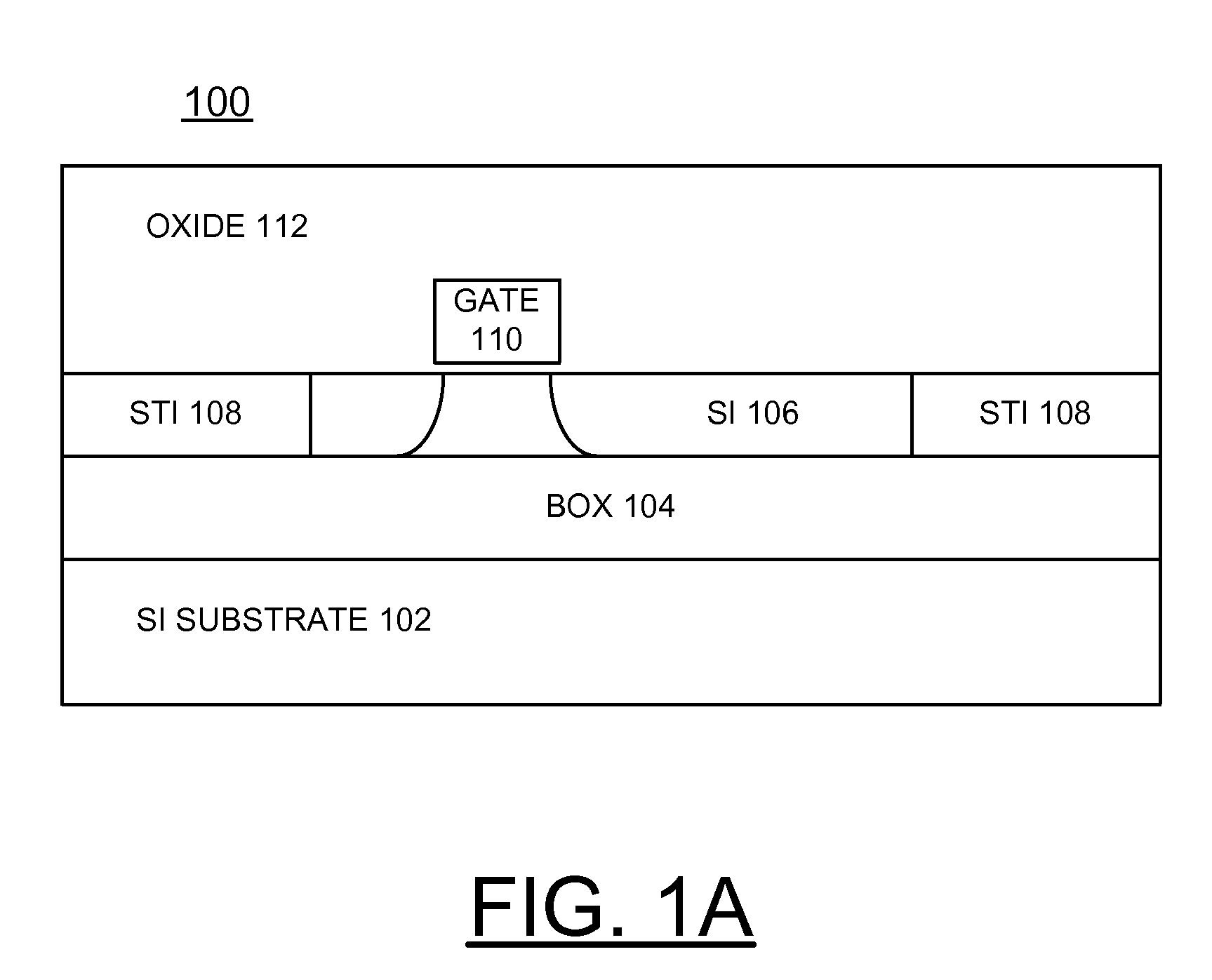
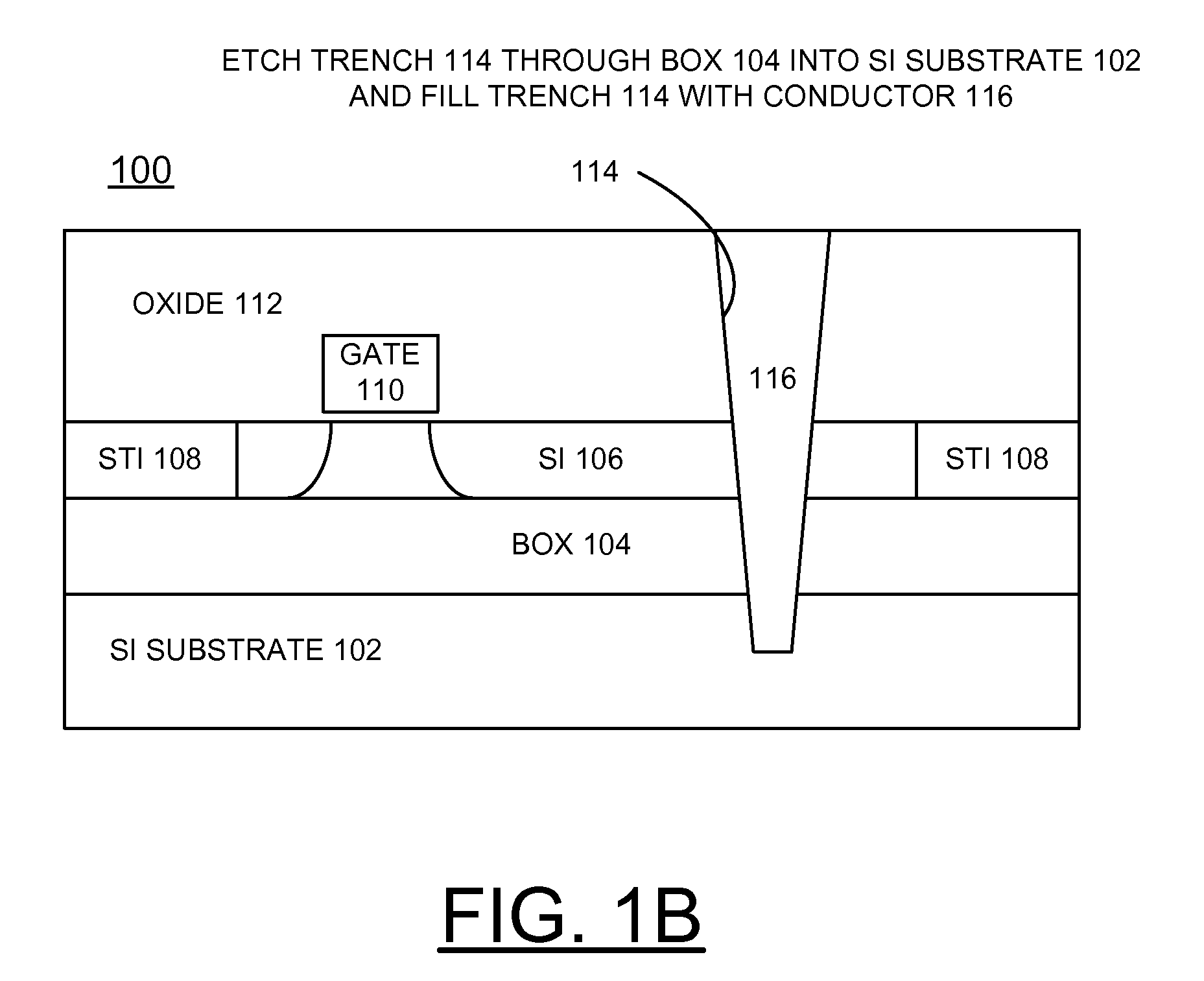
[0022]Having reference now to the drawings, FIGS. 1A, 1B, 1C, 1D, and 1E illustrate exemplary process steps for fabricating hotspot reduction structures in accordance with a preferred embodiment of the invention.

[0023]In FIG. 1A, there is shown an example silicon-on-insulator (SOI) structure 100 for implementing hotspot reduction structures in accordance with a first preferred embodiment of the invention. SOI structure 100 includes a silicon substrate layer 102, a thin buried oxide (BOX) layer 104 carried by the silicon substrate layer 102, an active layer 106 carried by the thin BOX ...


PUM


Abstract

Methods and structures are provided for implementing reduced hot spot thermal effects for silicon-on-insulator (SOI) circuits. A silicon-on-insulator (SOI) structure includes a silicon substrate layer, a thin buried oxide (BOX) layer carried by the silicon substrate layer, an active layer carried by the thin BOX layer, and a pad oxide layer carried by the active layer. A thermal conductive path is built to reduce thermal effects of a hotspot area in the active layer and extends from the active layer to the backside of the SOI structure. A trench etched from the topside to the active layer, and is filled with a thermal connection material. A thermal connection from a backside of the SOI structure includes an opening etched into the silicon substrate layer from the backside and filled with a thermal connection material.

Description

FIELD OF THE INVENTION[0001]The present invention relates generally to the field of manufacturing semiconductor devices, and more particularly, relates to a method and structures for implementing reduced hot spot thermal effects for silicon-on-insulator (SOI) circuits.DESCRIPTION OF THE RELATED ART[0002]Silicon-on-insulator (SOI) transistors provide better performance at low operating voltages than do transistors of similar dimensions fabricated in bulk silicon substrates. Superior performance of SOI transistors at low operating voltage is related to the relatively lower junction capacitances obtained on an SOI device as compared to a bulk silicon device of similar dimensions. A buried oxide (BOX) layer in an SOI device separates active transistor regions from the bulk silicon substrate, reducing junction capacitance.[0003]Typical semiconductor applications today have reached the point where the ability to keep the device junction temperatures under the limitations established for r...

Claims


Application Information

Patent Timeline
IPC IPC(8): H01L21/71H01L23/34
CPCH01L21/76898H01L21/84H01L23/3677H01L23/481H01L27/1203H01L29/78603H01L2924/0002H01L29/78606H01L29/78639H01L2924/00
Inventor BARTLEY, GERALD KEITHCHRISTENSEN, TODD ALANDAHLEN, PAUL ERICSHEETS, II, JOHN EDWARD
Owner IBM CORP
Why Eureka
Try Eureka