Schottky barrier integrated circuit

a technology of integrated circuits and shields, which is applied in the direction of semiconductor devices, electrical apparatus, transistors, etc., can solve the problems of reducing the effective switching speed of devices, and welch providing no indication that an actual cmos circuit was developed or fabricated

Inactive Publication Date: 2010-02-04
AVOLARE 2 LLC
View PDF15 Cites 1 Cited by
  • Summary
  • Abstract
  • Description
  • Claims
  • Application Information

AI Technical Summary

Problems solved by technology

The sub-linear Id-Vd turn-on characteristic of the SB-MOS device potentially reduces the effective switching speed of the device when used in an integrated circuit (IC).
However, Welch provides no indication that an actual CMOS circuit was developed or fabricated.

Method used


Image

  • Schottky barrier integrated circuit
  • Schottky barrier integrated circuit
  • Schottky barrier integrated circuit

Examples


Embodiment Construction

Overview

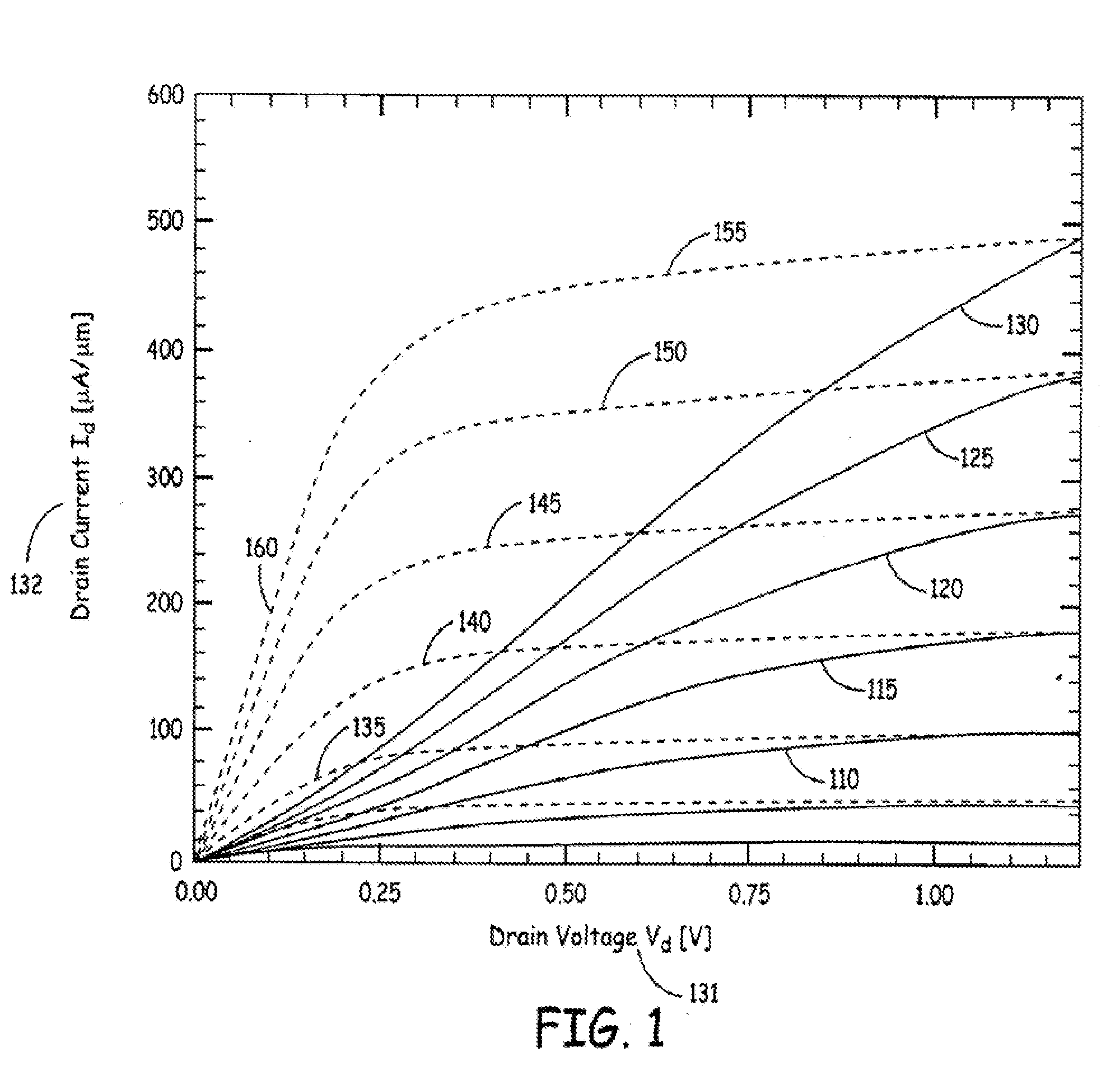
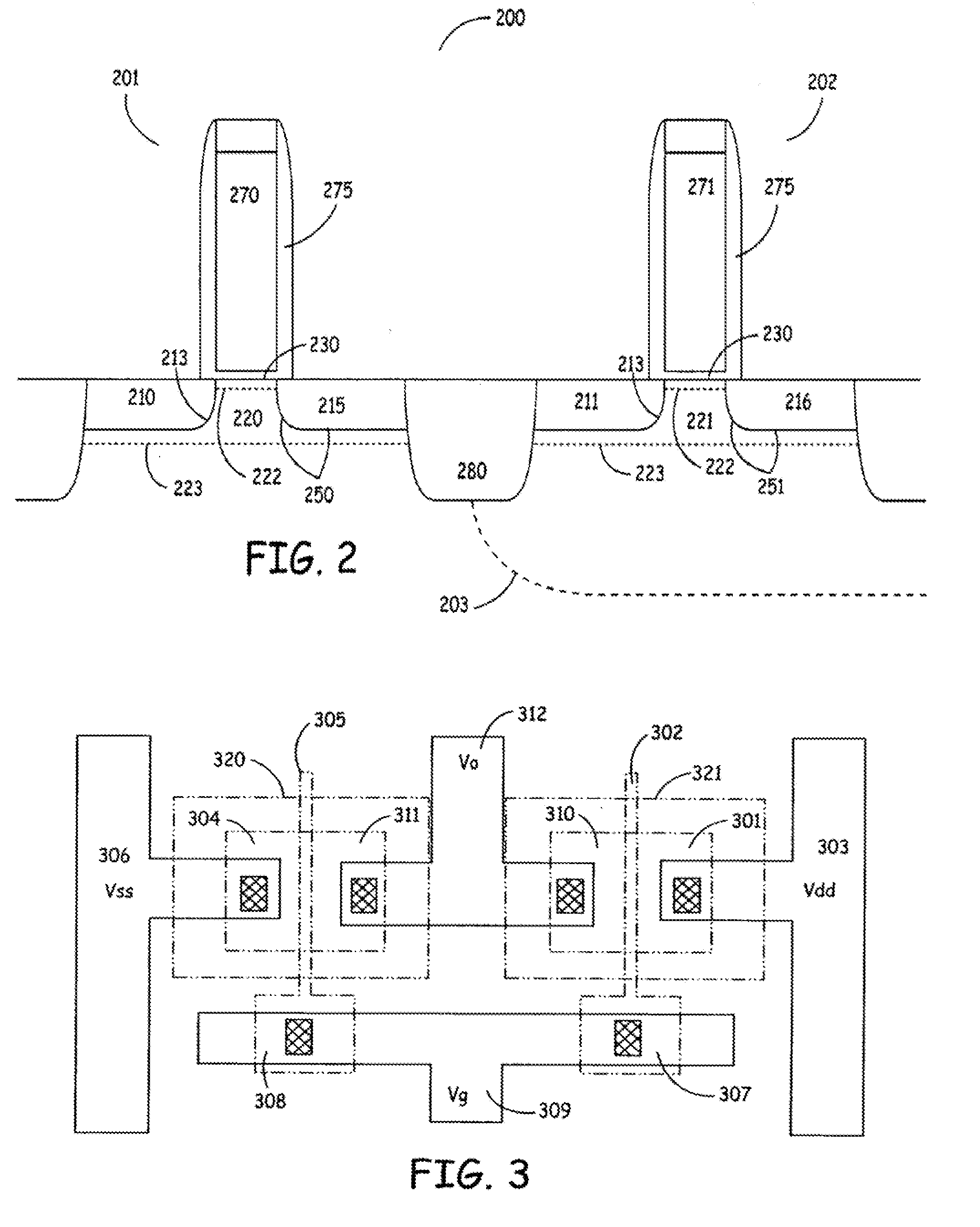
[0024]In general, the present invention provides an integrated circuit. The integrated circuit is generally comprised of at least one NMOS device or at least one PMOS device; wherein at least one of the NMOS devices or PMOS devices is a Schottky barrier MOS device with substantial bulk charge transport. In one embodiment, the Schottky barrier NMOS and Schottky barrier PMOS devices are each generally comprised of a semiconductor substrate and a gate electrode on the semiconductor substrate. The source electrode and a drain electrode on the semiconductor substrate define a channel region having a channel-length and having mobile charge carriers, wherein at least one of the source electrode and drain electrode forms a Schottky or Schottky-like contact to the substrate.

[0025]Of particular advantage, the inventors have discovered that the metal source and drain electrodes provide significantly reduced parasitic series resistance (˜10 Ω-μm) and contact resistance (less than 10−8 Ω...


PUM


Abstract

A Schottky barrier integrated circuit is disclosed, the circuit having at least one PMOS device or at least one NMOS device, at least one of the PMOS device or NMOS device having metal source-drain contacts forming Schottky barrier or Schottky-like contacts to the semiconductor substrate. The device provides a new distribution of mobile charge carriers in the bulk region of the semiconductor substrate, which improves device and circuit performance by lowering gate capacitance, improving effective carrier mobility μ, reducing noise, reducing gate insulator leakage, reducing hot carrier effect and improving reliability.

Description

CROSS-REFERENCE TO RELATED APPLICATIONS[0001]This is a continuation of U.S. patent application Ser. No. 10 / 944,627, filed on Sep. 17, 2004, which claimed benefit of and priority to U.S. Provisional Patent Application No. 60 / 504,078, filed Sep. 19, 2003, and claimed the benefit of and priority to U.S. Provisional Patent Application No. 60 / 556,046, filed Mar. 24, 2004, and claimed the benefit of and priority to U.S. Provisional Patent Application No. 60 / 577,685, filed Jun. 7, 2004. Each of the above provisional and non-provisional patent applications is incorporated by reference herein in its entirety.FIELD OF THE INVENTION[0002]The present invention generally relates to the field of semiconductor integrated circuits (ICs). More particularly, the present invention relates to ICs having Schottky barrier Metal-Oxide-Semiconductor-Field-Effect-Transistors (MOSFETs) including at least one Schottky barrier P-type MOSFETs (PMOS) or N-type MOSFETs (NMOS) and / or Schottky barrier complimentary...

Claims


Application Information

Patent Timeline
Patent Type & Authority Applications(United States)
IPC IPC(8): H01L29/78H01L27/088H01L21/336H01L21/8238H01L27/095
CPCH01L21/823814H01L29/7839H01L29/66643H01L27/095
Inventor SNYDER, JOHN P.LARSON, JOHN M.
Owner AVOLARE 2 LLC
Why Eureka
Try Eureka