Conductive bump, method for manufacturing the conductive bump, semiconductor device and method for manufacturing the semiconductor device

Active Publication Date: 2010-02-04
PANASONIC CORP
View PDF8 Cites 4 Cited by
  • Summary
  • Abstract
  • Description
  • Claims
  • Application Information

AI Technical Summary

Benefits of technology

[0035]Thus, it is possible to manufacture a semiconductor device that is excelle

Problems solved by technology

In this case, as the pitches of electrode terminals are narrowed, a short circuit between neighboring connection terminals on a mounting board occurs and a connection failure easily occurs between a conductive bump and an electrode terminal by stress that may be generated due to a difference in the thermal expansion coefficient between the semiconductor element and the mounting board.
In particular, the above-mentioned mobile electronic devices such as portable telephones may undergo shock when they are dropped.
Therefore, when connection reliability between electrode terminals is insufficient, failure of the mobile electronic device may occur.
Therefore, when an Au bump and the like is

Method used


Image

  • Conductive bump, method for manufacturing the conductive bump, semiconductor device and method for manufacturing the semiconductor device
  • Conductive bump, method for manufacturing the conductive bump, semiconductor device and method for manufacturing the semiconductor device
  • Conductive bump, method for manufacturing the conductive bump, semiconductor device and method for manufacturing the semiconductor device

Examples


Example

First Exemplary Embodiment

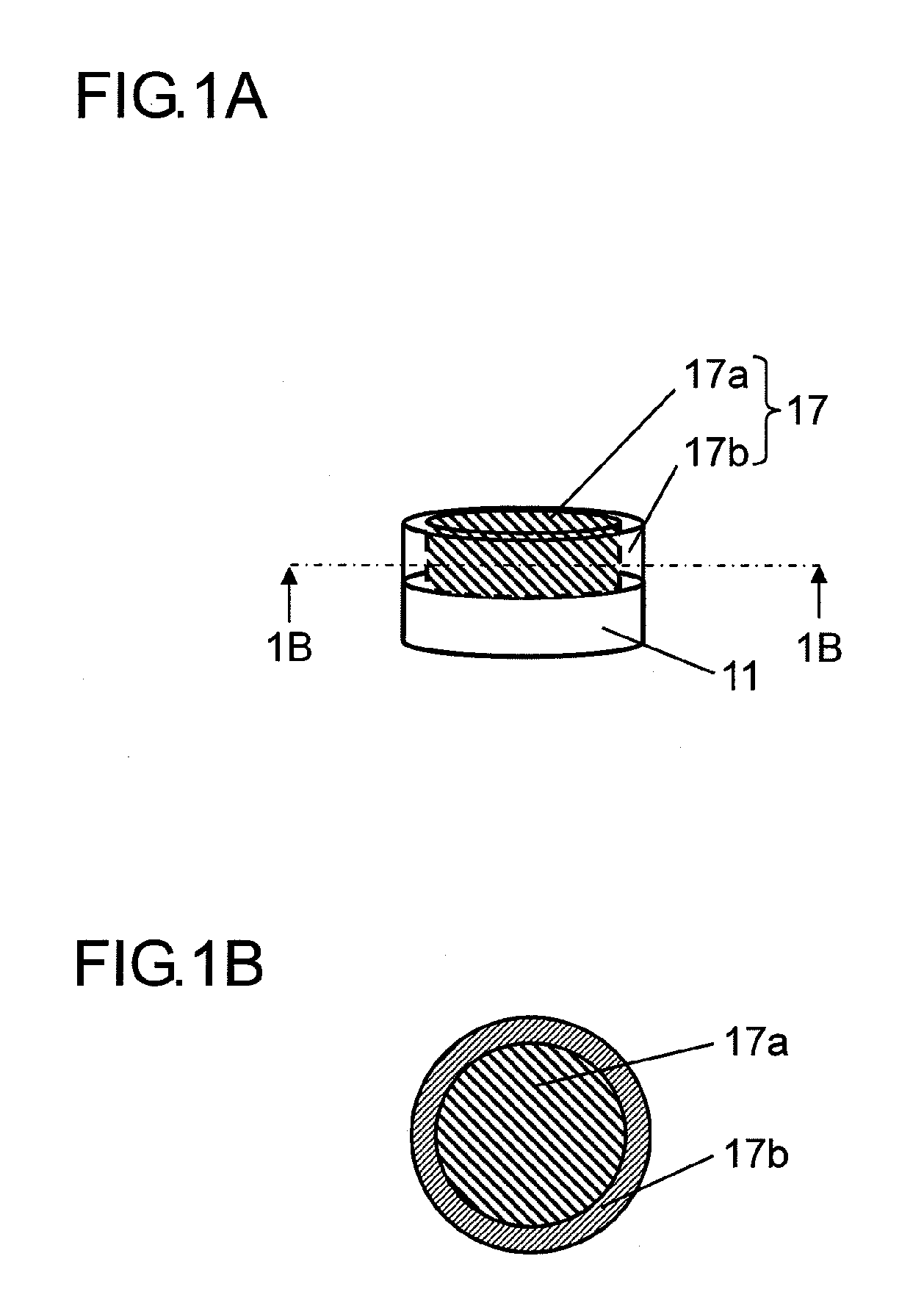
[0080]FIG. 1A is a perspective view conceptually illustrating a structure of a conductive bump in accordance with a first exemplary embodiment of the present invention, and FIG. 1B is a cross-sectional view taken on line 1B-1B of FIG. 1A. In FIGS. 1A and 1B, an electronic component on which a conductive bump is formed is not shown.

[0081]As shown in FIGS. 1A and 1B, conductive bump 17 formed on electrode terminal 11 of an electronic component (not shown) including, for example, a semiconductor element, a circuit board, and the like, is composed of, for example, first cured portion 17a and second cured portion 17b. First cured portion 17a is formed in the center portion of conductive bump 17 and cured by a photo-curing method and a thermal curing method. Second cured portion 17b is formed so as to surround first cured portion 17a on the outer periphery of electrode terminal 11 and is semi-cured in a prepreg state by a thermal curing method. Conductive bump 17...

Example

Second Exemplary Embodiment

[0106]Hereinafter, a structure of a conductive bump in accordance with a second exemplary embodiment of the present invention is described with reference to FIGS. 4A to 4C.

[0107]FIG. 4A is a cross-sectional view illustrating a structure of a conductive bump in accordance with the second exemplary embodiment of the present invention. FIG. 4B is a cross-sectional view illustrating another example of a structure of a conductive bump in accordance with the second exemplary embodiment of the present invention. FIG. 4C is a cross-sectional view illustrating a yet another example of a structure of a conductive bump in accordance with the second exemplary embodiment of the present invention.

[0108]As shown in FIGS. 4A to 4C, the basic structure includes first cured portion 37a and second cured portion 37b having different densities of conductive filler constituting a conductive bump, which are laminated on, for example, semiconductor wafer 32 in the direction of th...

Example

Third Exemplary Embodiment

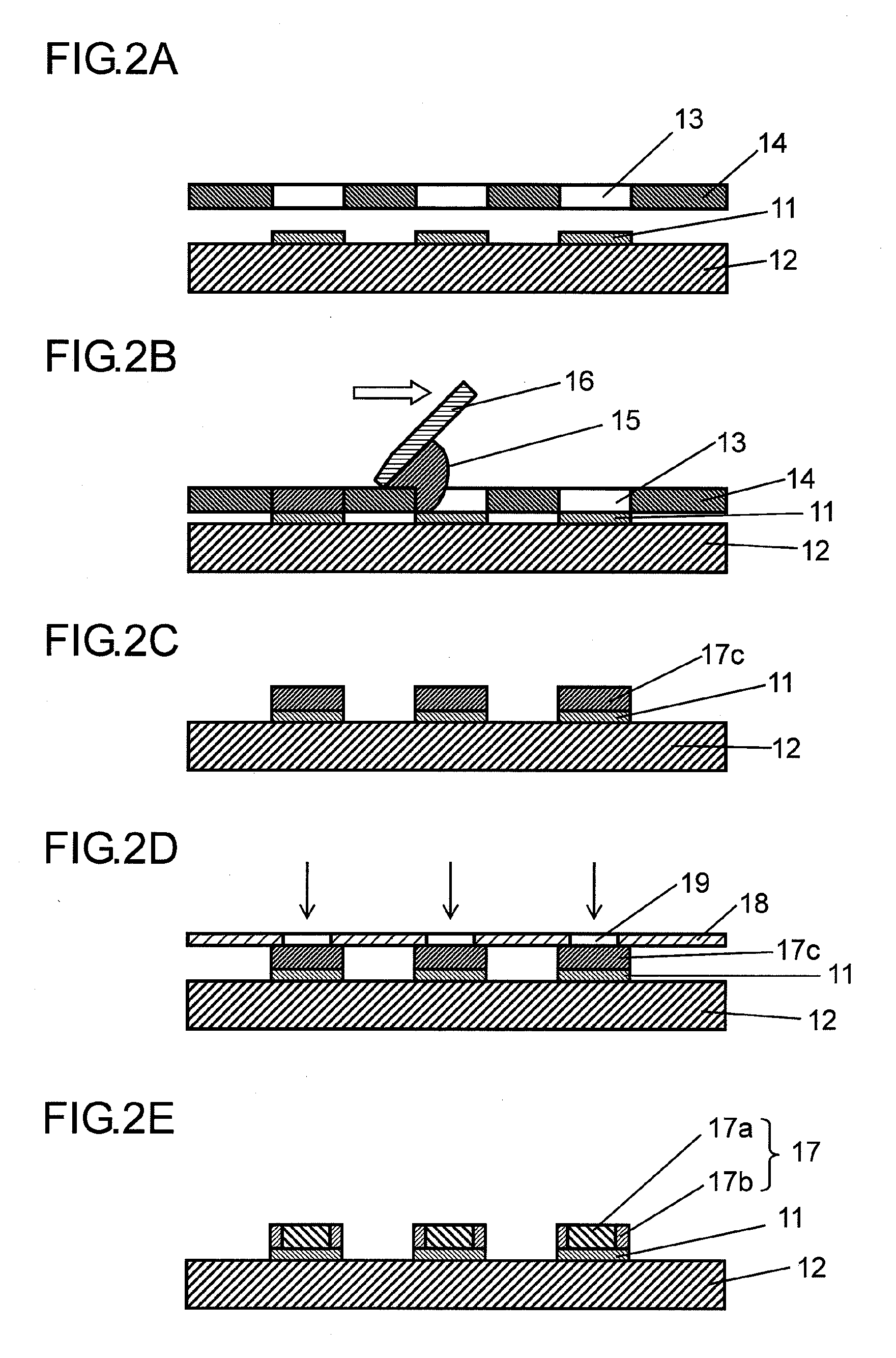
[0113]Hereinafter, a method for forming a conductive bump in accordance with a third exemplary embodiment of the present invention is described with reference to FIGS. 5A to 5E. FIGS. 5A to 5E are cross-sectional views illustrating a method for forming a conductive bump in accordance with the third exemplary embodiment of the present invention. Similar to the case in the first exemplary embodiment, an example in which a semiconductor wafer having a large number of semiconductor elements as an electronic component to be provided with a conductive bump is formed described. Furthermore, an example in which a liquid crystal mask is used as an exposure mask is described. However, a metal mask may be used.

[0114]Firstly, as shown in FIG. 5A, on the upper surface of semiconductor wafer 42 having a plurality of semiconductor elements on which a plurality of electrode terminals 41 are formed, print mask 44 having openings 43 for forming conductive bumps corresponding...


PUM


Abstract

Conductive bump (17) formed on a surface of electrode terminal (11) of an electronic component. Conductive bump (17) is composed of at least a plurality of cured resin materials having different conductive filler densities. Thus, a short circuit and a connection failure due to crush of conductive bump (17) at the time of mounting can be prevented.

Description

TECHNICAL FIELD[0001]The present invention relates to a conductive bump formed on an electrode terminal of a semiconductor element or an electrode terminal of a circuit board. More particularly, the present invention relates to a semiconductor device in which semiconductor elements having narrow-pitched electrode terminals are reliably mounted on electrode terminals of a circuit board.BACKGROUND ART[0002]Recently, in mobile electronic devices such as portable telephones, notebook-sized personal computers, PDAs and digital video cameras, which have been rapidly widespread, technology development for realizing small, thin and light devices has been rapidly advanced.[0003]One principle electronic component for supporting this technology development is a semiconductor element. As the density of semiconductor elements is increased, the pitches and areas of electrode terminals have been reduced. Accordingly, strict requirements have been made with respect to a conductive bump used in flip...

Claims


Application Information

Patent Timeline
IPC IPC(8): H01L21/50H01L23/498H01B5/00B05D3/06
CPCH01L2924/01057H01L2224/13078H01L2924/01078H01L2924/01079H01L2924/01082H01L21/563H01L24/11H01L24/12H01L24/16H01L24/83H01L2224/1132H01L2224/11552H01L2224/13099H01L2224/1319H01L2224/16H01L2224/83851H01L2924/01015H01L2924/01029H01L2924/01033H01L2924/01042H01L2924/01046H01L2924/01047H01L2924/01005H01L2924/01006H01L2924/014H01L2224/1131H01L2924/00013H01L2924/01074H01L2224/13076H01L2224/1329H01L2224/2919H01L2224/13339H01L2924/3512H01L2924/00H01L2924/00014H01L2224/29099H01L2224/131H01L2224/05573H01L2224/05568H01L2224/0554H01L2224/05599H01L2224/0555H01L2224/0556
Inventor YAGI, YOSHIHIKOSAKURAI, DAISUKE
Owner PANASONIC CORP
Why Eureka
Try Eureka