Ceramic chip substrate for microwave integrated circuit and manufacturing method thereof

A microwave integrated circuit and manufacturing method technology, applied in circuits, electrical components, electrical solid devices and other directions, can solve the problems of uneven pads, uneven chip mounting, large grounding resistance, etc., and achieve high chip mounting density, satisfying Heat dissipation requirements and good process compatibility

Pending Publication Date: 2021-03-09
NO 43 INST OF CHINA ELECTRONICS TECH GRP CETC
View PDF0 Cites 0 Cited by
  • Summary
  • Abstract
  • Description
  • Claims
  • Application Information

AI Technical Summary

Problems solved by technology

[0003] The existing chip substrate grounding circuit for microwave integrated circuits is mainly manufactured by thin film evaporation sputtering metal conductive layer process or electroplating / electroless plating process. In actual placement, there is a large grounding resistance, and the conductive glue or solder at the bottom of the chip substrate overflows from the light-transmitting through hole to the upper surface of the substrate, which makes the chip mounting pad uneven, resulting in uneven chip mounting.
[0004] Some civilian chip substrates are made by using thick film technology to bury silver vias in the alumina ceramic substrate, but the thermal conductivity of the alumina ceramic substrate is low (not greater than 20W / m·K), which cannot provide high-power chips. The problem with good cooling
Moreover, the silver conductor is easy to oxidize and easy to produce "silver migration", which does not completely match the gold wire bonding assembly process of the chip, so that the chip substrate cannot work for a long time under harsh conditions, and cannot be used for high-reliability and high-power microwave integrated circuit packaging

Method used


Image

  • Ceramic chip substrate for microwave integrated circuit and manufacturing method thereof
  • Ceramic chip substrate for microwave integrated circuit and manufacturing method thereof
  • Ceramic chip substrate for microwave integrated circuit and manufacturing method thereof

Examples


Embodiment 1

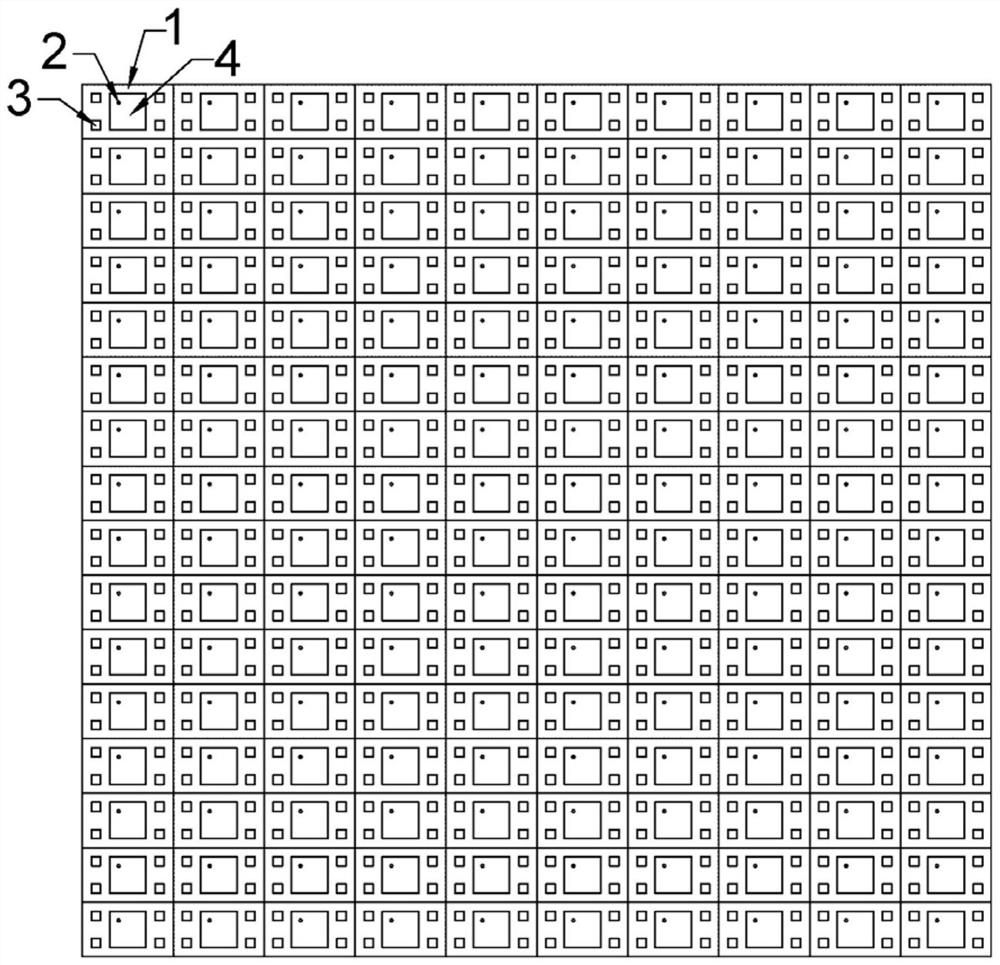
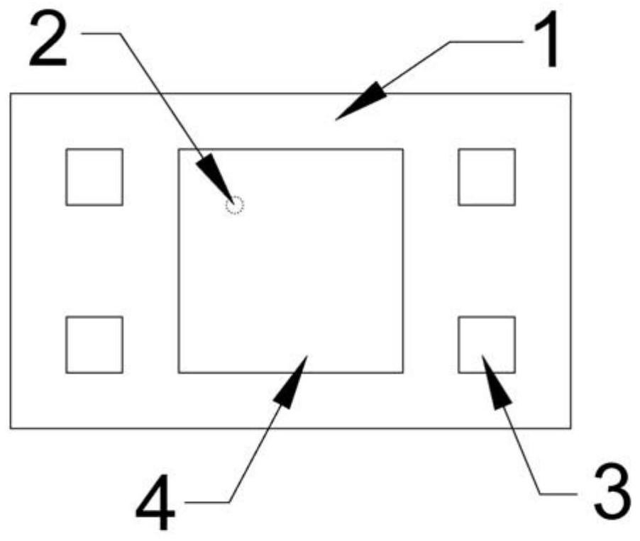
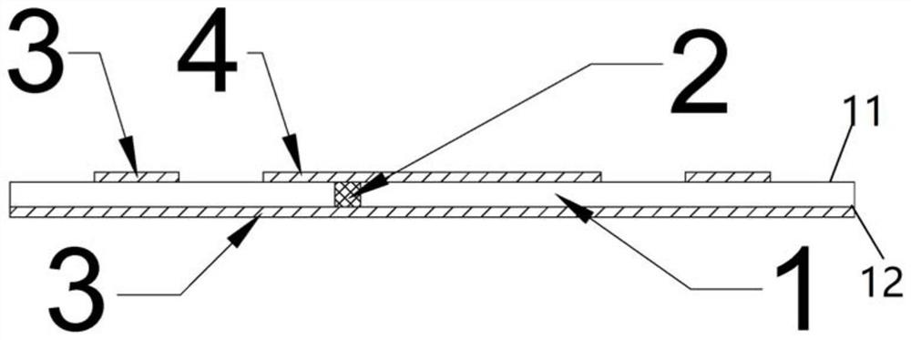
[0060] see figure 1 , in this embodiment, the aluminum nitride ceramic substrate 1 (aluminum nitride ceramic substrate with a thermal conductivity ≥ 170 W / m·K and a purity of not less than 95%) has a thickness of 0.25 mm, and both length and width are 51 mm. On the aluminum nitride ceramic substrate 1, 16 rows and 10 columns of 160 single-chip substrate designs are arrayed in a square area with a size of 50mm×50mm. The size of the designed ceramic chip substrate is 5mm×3mm. The design graphics are as follows: figure 2 and image 3 shown.

[0061] according to figure 1 In the array arrangement pattern shown, 160 light-transmitting through holes with a diameter of 0.08 mm are produced on the aluminum nitride ceramic substrate 1 by means of laser drilling.

[0062] Next, after the gold powder paste is filled in the light-transmitting through-holes by screen printing, the aluminum nitride ceramic substrate 1 is sintered at 850° C. for 5 minutes, so that the gold powder paste i...

Embodiment 2

[0067] First, if Figure 5 As shown, in this embodiment, the aluminum nitride ceramic substrate 1 (thermal conductivity ≥ 170W / m·K, purity not less than 95%) has a thickness of 0.38mm, a length and a width of 101.6mm, and its size is 100mm A total of 100 ceramic chip substrate design patterns are arranged in an array of 10 rows and 10 columns in a square area of ​​×100mm. The size of each small-sized ceramic chip substrate is 10mm×10mm, and its design graphics are as follows Figure 5 , Figure 6 , Figure 7 shown.

[0068] according to Figure 5 In the array arrangement pattern shown, 1700 light-transmitting through holes with a diameter of 0.1 mm are produced on the aluminum nitride ceramic substrate 1 by means of laser drilling.

[0069] Next, fill the gold powder paste in the light-transmitting through hole by screen printing, and sinter at 850° C. for 5 minutes. The gold powder paste in the through hole of the aluminum nitride ceramic substrate 1 forms 1700 gold cond...


PUM

PropertyMeasurementUnit
thicknessaaaaaaaaaa
diameteraaaaaaaaaa
thicknessaaaaaaaaaa

Abstract

The invention discloses a ceramic chip substrate for a microwave integrated circuit and a manufacturing method of the ceramic chip substrate; the ceramic chip substrate comprises an aluminum nitride ceramic substrate provided with a plurality of through holes, gold conductive columns are embedded in the through holes, the diameters of the gold conductive columns are equal to the inner diameters ofthe through holes, and the heights of the gold conductive columns are equal to the thickness of the aluminum nitride ceramic substrate; the surface of the aluminum nitride ceramic substrate is provided with a thick film gold conductor chip mounting pad and a thick film gold conductor circuit pattern. The ceramic chip substrate for the microwave integrated circuit is small in on-resistance betweenthe surfaces, high in heat conductivity, simple in manufacturing process, suitable for two micro-assembly processes of adhesive bonding and gold wire bonding on the surface at the same time, and capable of being used for packaging a high-reliability high-power microwave integrated circuit.

Description

technical field [0001] The invention belongs to the technical field of microwave integrated circuit packaging, and in particular relates to a ceramic chip substrate for microwave integrated circuits, and also relates to a manufacturing method of the ceramic chip substrate. Background technique [0002] Chip submount (chip submount) is a component in microwave integrated circuits, generally located between the chip and the package shell or between the chip and the printed circuit board, which mainly plays the role of support, heat dissipation, improvement of thermal mismatch, and electrical connection. [0003] The existing chip substrate grounding circuit for microwave integrated circuits is mainly manufactured by thin film evaporation sputtering metal conductive layer process or electroplating / electroless plating process. In actual placement, there is a large grounding resistance, and the conductive glue or solder at the bottom of the chip substrate overflows from the light...

Claims


Application Information

Patent Timeline
Patent Type & Authority Applications(China)
IPC IPC(8): H01L21/48H01L23/48H01L23/498H01L23/15
CPCH01L21/4821H01L23/15H01L23/481H01L23/49816H01L23/49838
Inventor 刘俊永吴建利王伟
Owner NO 43 INST OF CHINA ELECTRONICS TECH GRP CETC
Why Eureka
Try Eureka