Thermoelectric module and metallized substrate

a technology of thermoelectric modules and metalized substrates, which is applied in the direction of thermoelectric devices with peltier/seeback effects, electrical apparatus, and semiconductor laser mounting devices, etc., can solve the problems of melting of thermoelectric elements, etc., to achieve the effect of reducing the cross-sectional area of thermoelectric elements and breaking of elements

Inactive Publication Date: 2010-02-11
KELK LTD
View PDF2 Cites 4 Cited by
  • Summary
  • Abstract
  • Description
  • Claims
  • Application Information

AI Technical Summary

Benefits of technology

[0015]As described above, with the thermoelectric device substrate and the thermoelectric device according to the present invention, the breakage of the elements caused by thermal stress generated during assembly or during pre-tinning performed to attach a package or an object to be cooled can be reduced even in a case of a thermoelectric module in which the cross-sectional area of thermoelectric elements becomes smaller and thus the element occupying area ratio is 40% or less. This makes it possible to meet requirements for further reduction of power consumption.

Problems solved by technology

However, since the cross-sectional area of the thermoelectric elements becomes smaller in a downsized and power-saving thermoelectric module as described above, the mechanical strength of the thermoelectric elements decreases.
Moreover, the cooling-side surface area of the upper metalized substrate of the thermoelectric module for mounting a semiconductor laser cannot be made smaller in view of assembling workability and so on.
This induces a problem of breakage of the thermoelectric elements caused by thermal stress generated during assembly, or during pre-tinning performed for attaching a package or an object to be cooled.

Method used


Image

  • Thermoelectric module and metallized substrate
  • Thermoelectric module and metallized substrate
  • Thermoelectric module and metallized substrate

Examples


examples

[0031]A manufacturing method of the thermoelectric module according to the present invention will be described.

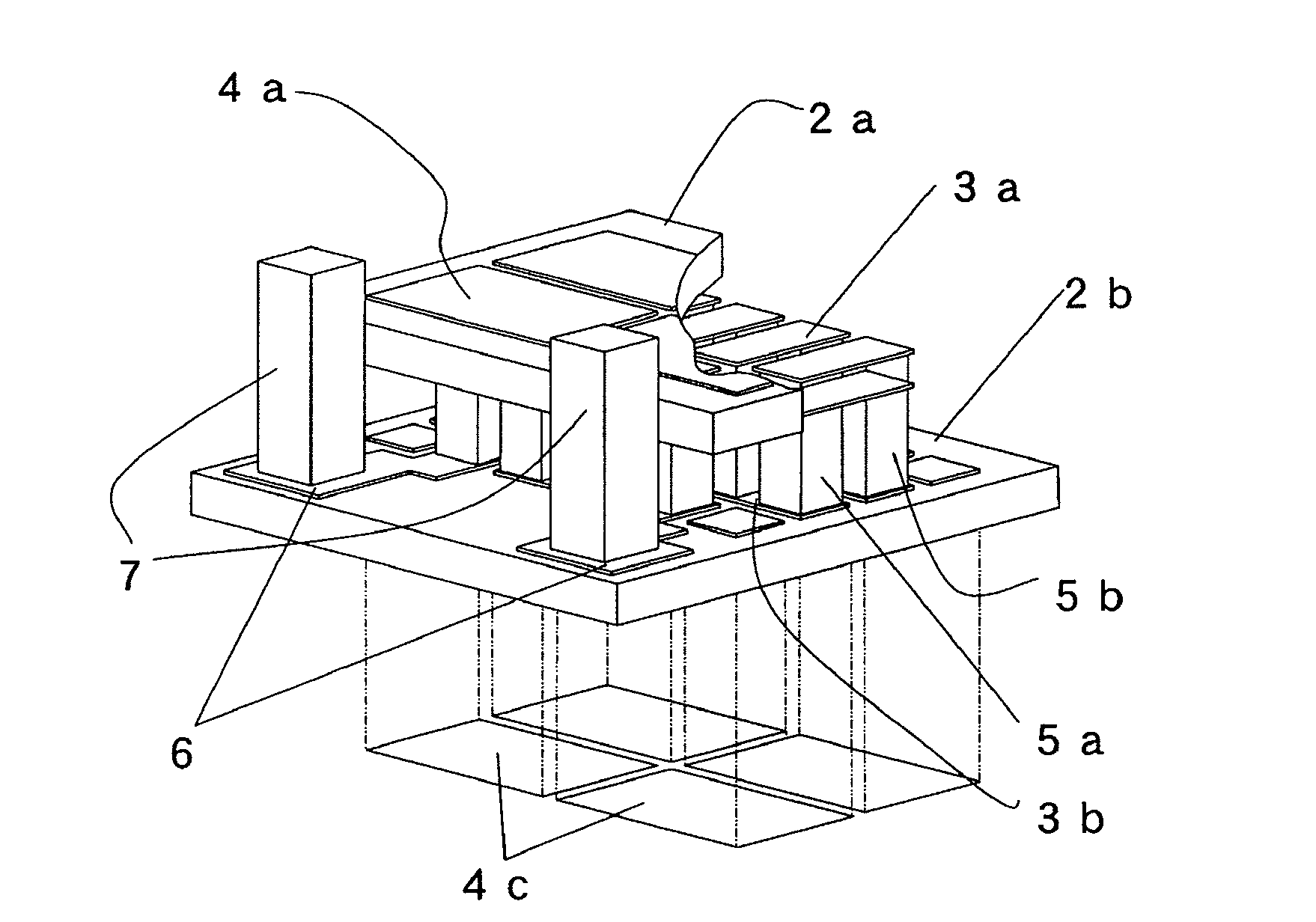
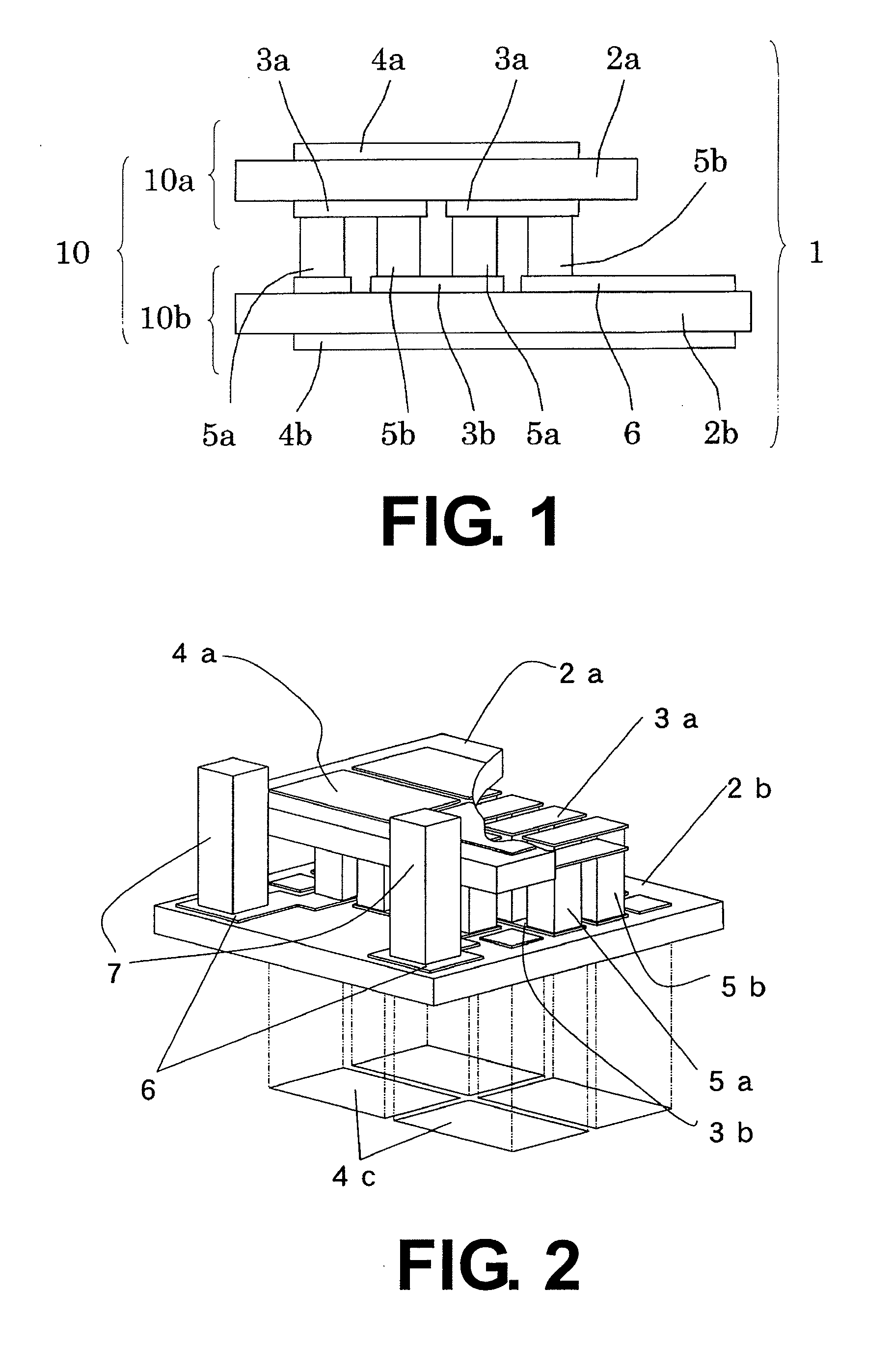
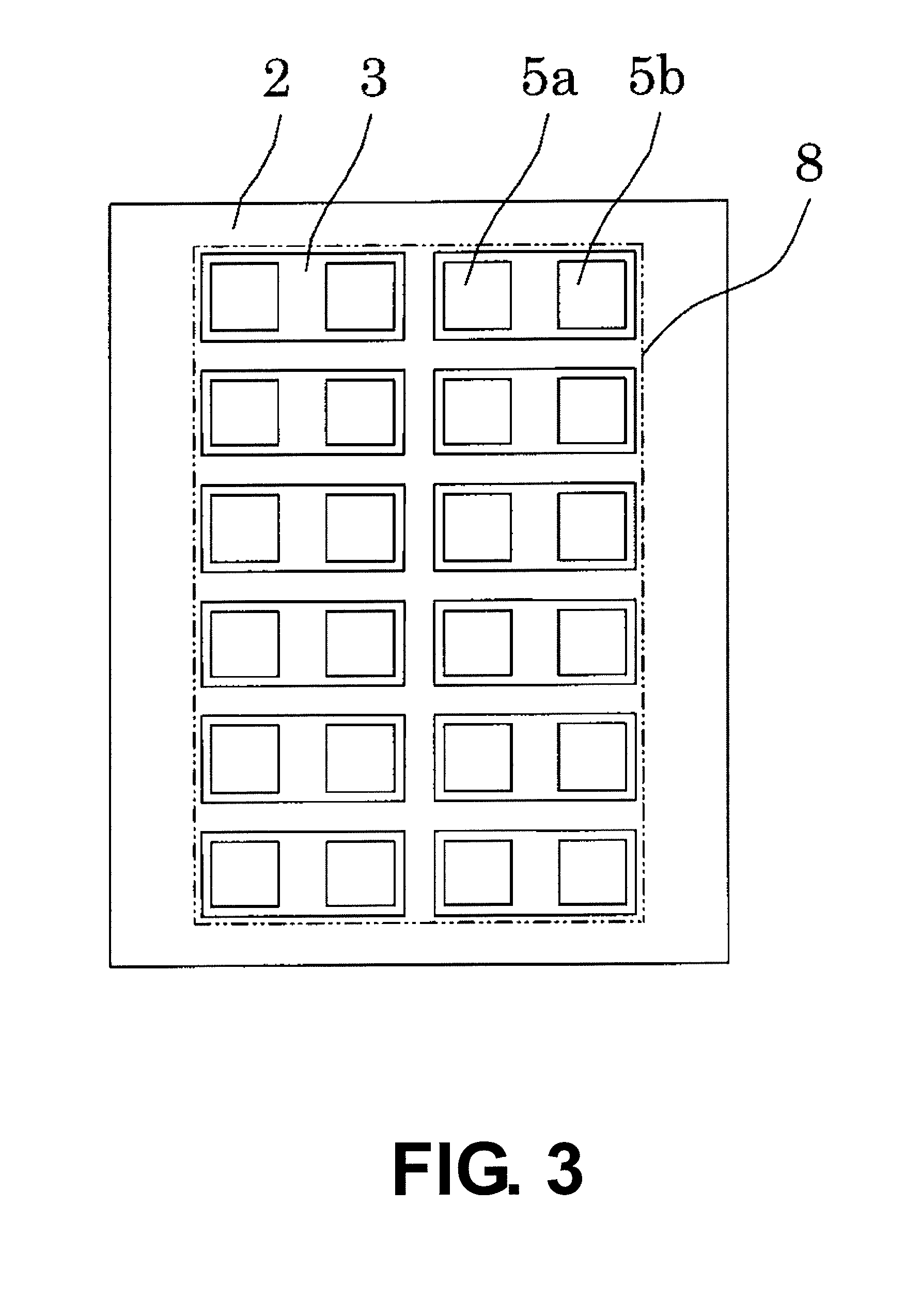
[0032]Alumina was used as an insulating substrate and a metalized layer comprising three layers of Cu / Ni / Au was formed thereon in a desired shape by plating, thermal spraying or the like.

[0033]Bi—Te thermoelectric elements were then bonded to the surfaces of metal electrodes on the metalized substrate with the use of AuSn solder which was heated to a temperature equal to or higher than the melting point (280° C.) of the solder, whereby a thermoelectric module was manufactured.

[0034]A visual test was conducted on the thermoelectric modules thus obtained with the use of a microscope with a magnification of 200× to examine the thermoelectric elements. The number of thermoelectric modules in which cracks were observed in the thermoelectric elements was counted to calculate the rate of defectives with cracked elements represented by the expression [the number of thermoelectric m...


PUM


Abstract

A thermoelectric module (1) utilizing the Peltier effect, exhibiting an element-occupied area ratio of 40% or below, the element-occupied area ratio defined as the ratio of the sum of cross-sectional areas, perpendicular to the direction of electric current passage, of thermoelectric elements (5a,5b) to the area of insulating substrate (2a) being in contact with an object to be cooled via a metalized layer (4a), wherein metalized layers (4a,4b) are provided with slits. In this construction, there can be prevented breakage of thermoelectric device by thermal stress occurring at assembly, or thermal stress occurring at pre-tinning conducted in advance for attaching an object to be cooled or at attaching package, etc.

Description

TECHNICAL FIELD[0001]The present invention relates to a thermoelectric module substrate utilizing the Peltier effect for use in thermoelectric conversion such as heat absorption or cooling, and also relates to a thermoelectric module using the substrate.BACKGROUND ART[0002]Thermoelectric modules utilizing the Peltier effect are simple in configuration and easy to reduce the size and weight thereof. Furthermore, they are operable without noise and vibration, and their accuracy and response are very high. Therefore, these thermoelectric modules are applied in various fields, including temperature controllers in semiconductor devices such as semiconductor lasers, and semiconductor manufacturing equipment. A thermoelectric module has a plurality of thermoelectric elements arrayed on a substrate. FIG. 1 is a side view showing a thermoelectric module used, for example, for temperature control of a semiconductor laser. This thermoelectric module 1 has two insulating substrates 2a and 2b ar...

Claims


Application Information

Patent Timeline
Patent Type & Authority Applications(United States)
IPC IPC(8): H01L35/28
CPCH01L35/04H01L35/08H01L35/32H01L2924/0002H01L2924/00H10N10/817H10N10/81H10N10/17
Inventor KINOSHI, AKIOYAMANASHI, MASATAKAHAJIME, HIROFUMIFUJIKAWA, SHINGO
Owner KELK LTD
Why Eureka
Try Eureka