Apparatus for Holding Semiconductor Wafers

a technology for semiconductor wafers and apparatuses, applied in liquid surface applicators, coatings, chemical vapor deposition coatings, etc., can solve the problems of wafer substrates losing direct abutting contact with mounting surfaces, conventional electrostatic chucks,

Inactive Publication Date: 2010-02-11
TAIWAN SEMICON MFG CO LTD
View PDF7 Cites 44 Cited by
  • Summary
  • Abstract
  • Description
  • Claims
  • Application Information

AI Technical Summary

Benefits of technology

[0008]These and other problems are generally solved or circumvented, and technical advantages are generally achieved, by preferred embodiments of the present invention. The preferred embodiments provide a wafer holding apparatus that comprises a heat-conductive layer disposed on a supporting base, and a plurality of heat-conductive lift pins coupled to a heating

Problems solved by technology

Conventional electrostatic chucks, however, have the following problems.
This problem causes the wafer substrate 18 to lose direct abutting contact with the mounting surface 15 where the bowing or warping occurs.
This causes further temperature non-uniformity in wafer substrate 18.
Additionally, for the system where alternating voltage is applied to the electrodes 12, electric charge is accumulated in the back surface of wafer substrate 18 while the wafer is being attracted, and the accumulated charge makes the separation of the substrate from the chuck difficult.
Moreover, althou

Method used


Image

  • Apparatus for Holding Semiconductor Wafers
  • Apparatus for Holding Semiconductor Wafers
  • Apparatus for Holding Semiconductor Wafers

Examples


Embodiment Construction

[0018]The making and using of the presently preferred embodiments are discussed in detail below. It should be appreciated, however, that the present invention provides many applicable inventive concepts that can be embodied in a wide variety of specific contexts. The specific embodiments discussed are merely illustrative of specific ways to make and use the invention, and do not limit the scope of the invention.

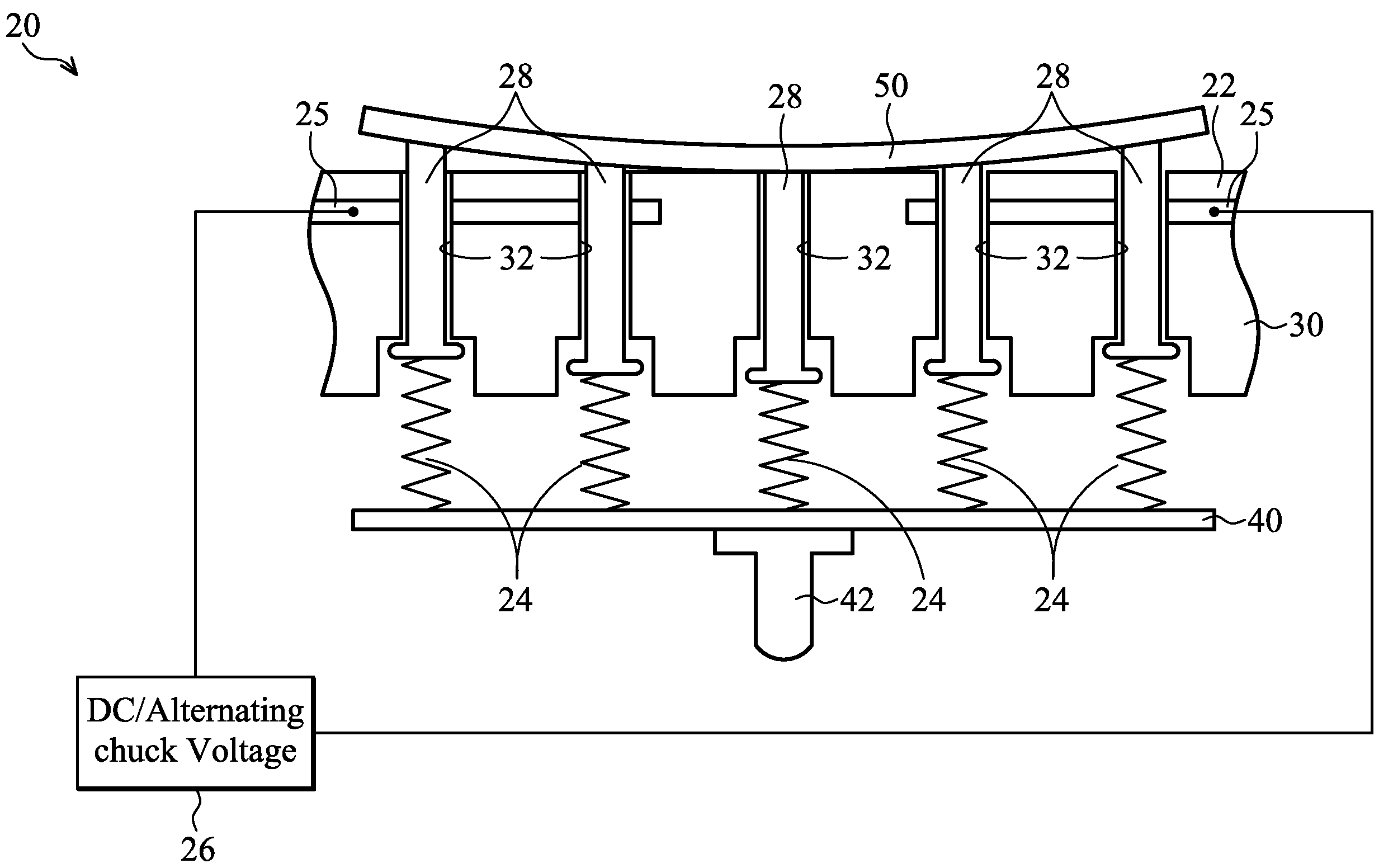
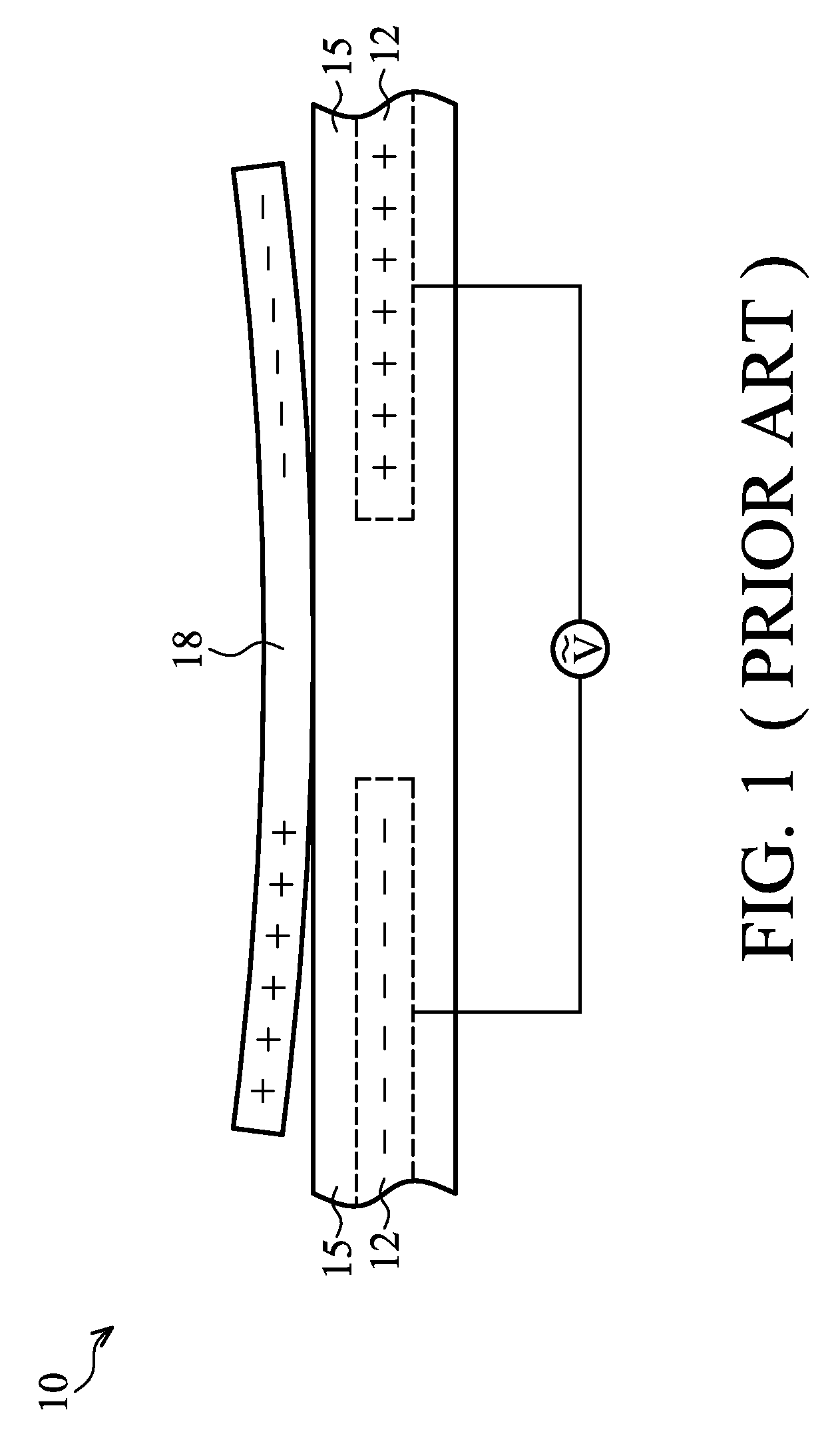
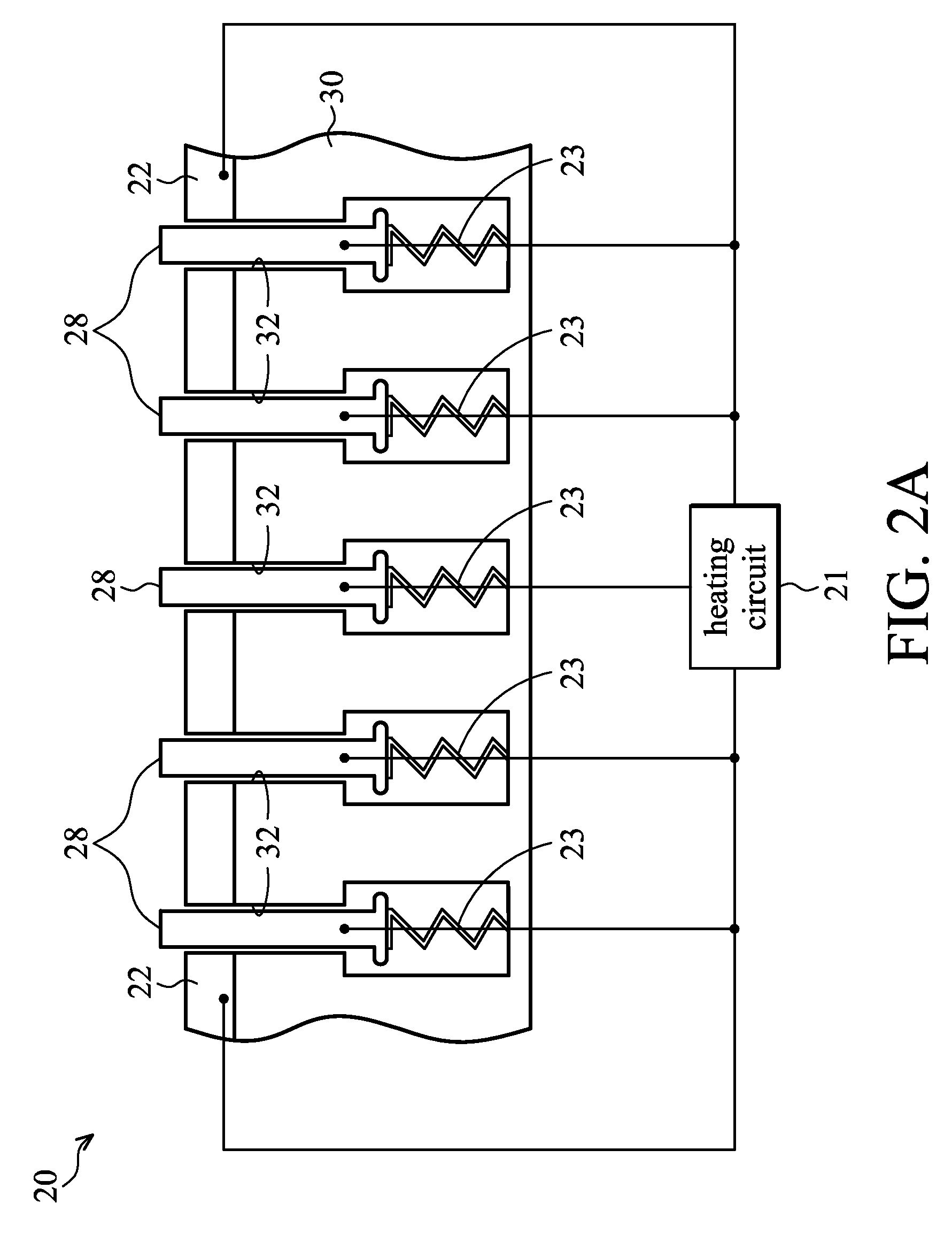
[0019]The present invention will be described with respect to preferred embodiments in a specific context, namely wafer holding apparatus and methods that realize even temperature distribution in a wafer substrate during processes involving elevated wafer temperature, such as chemical vapor deposition (CVD), impurity doping, rapid thermal process (RTP), anneal, and metal deposition. Preferred embodiments may be used to heat wafer substrates of various diameter, achieving even temperature distribution across a wafer substrate to perform desired processes. Also, preferred embod...


PUM

PropertyMeasurementUnit
Temperatureaaaaaaaaaa
Diameteraaaaaaaaaa
Electrical conductoraaaaaaaaaa

Abstract

Apparatus for holding semiconductor wafers during semiconductor manufacturing processes are disclosed. In one embodiment, the apparatus comprises a heat-conductive layer disposed on a supporting base. The apparatus also comprises a plurality of holes formed through the heat-conductive layer and the supporting base. The apparatus further comprises a plurality of heat-conductive lift pins that extend through the holes over the heat-conductive layer at the top end, and make a direct contact with a wafer substrate. The heat-conductive layer and the lift pins are connected to a heating circuit.

Description

CROSS-REFERENCES[0001]This application claims the benefit of the following provisionally filed U.S. patent application Ser. No. 61 / 087,468, filed Aug. 8, 2008, and entitled “Apparatus for Holding Semiconductor Wafers,” which application is hereby incorporated herein by reference.TECHNICAL FIELD[0002]The present invention relates generally to an apparatus for holding semiconductor wafers during semiconductor manufacturing processes, and more particularly to wafer holding apparatus and methods that realize wafer temperature uniformity in processes with high heat stress.BACKGROUND[0003]Manufacturing a semiconductor integrated circuit (IC) typically involves numerous processing techniques that require elevated wafer temperatures to perform the desired processes, such as chemical vapor deposition (CVD), physical vapor deposition (PVD), dry etching, or other processing techniques. As a known wafer holding apparatus, an electrostatic chuck including a heating element is commonly employed t...

Claims


Application Information

Patent Timeline
IPC IPC(8): C23F1/08C23C16/46
CPCH01L21/67103H01L21/6833H01L21/68742H01L21/6831C23C16/4585H01L21/68721H01L21/68728H01L21/6875
Inventor YU, CHEN-HUAHWANG, CHIEN LING
Owner TAIWAN SEMICON MFG CO LTD
Why Eureka
Try Eureka