

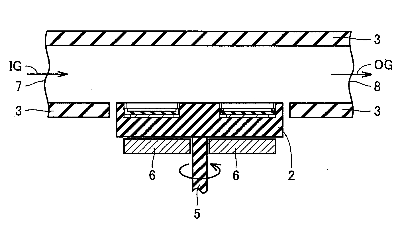
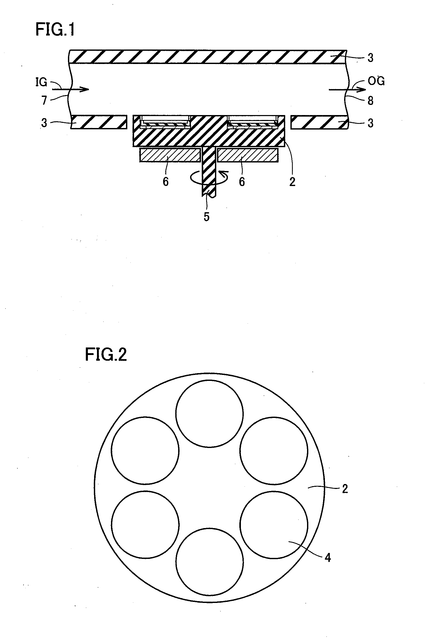
Fabrication apparatus and fabrication method of semiconductor device produced by heating substrate
a technology of fabrication apparatus and substrate, which is applied in the direction of semiconductor devices, chemical vapor deposition coatings, coatings, etc., can solve the problem that the heat from the heater member located at the back side of the susceptor cannot be readily conveyed to the support portion of the support member, and achieve the effect of uniform temperature distribution of the substra
- Summary
- Abstract
- Description
- Claims
- Application Information
AI Technical Summary
Benefits of technology
Problems solved by technology
Method used
Image

Examples
example 3
Conventional Example 3
[0076]The temperature distribution at the surface of substrate 1 in the case where quartz ring 211 of Conventional Example 2 was inserted was obtained by the radiation heat transfer simulation. Based on an axisymmetric model as shown in FIG. 16, a two-dimensional simulation was performed in relation to substrate 1 for a length (25 mm) corresponding to the radius thereof. The dimension of susceptor 202 in the direction corresponding to the radial direction of substrate 1 was 30 mm, and in the direction corresponding to the thickness direction of substrate 1 was 7.6 mm. The thickness of substrate 1 was 0.35 mm. The width (dimension in the radial direction of substrate 1) and the thickness (dimension in the thickness direction of substrate 1) of quartz ring 211 was 1.0 mm and 0.2 mm, respectively. The side of susceptor 202 at the back side was set constant at 1000° C., and the side corresponding to the outer circumferential side of susceptor 202 was heat-insulated...
example 1
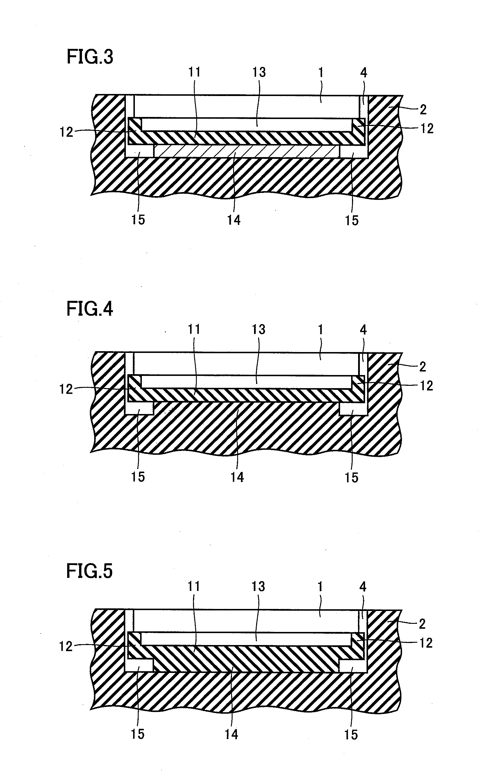
[0079]The temperature distribution at the surface of substrate 1 corresponding to the configuration of support member 11 and spacer 14 of FIG. 3 was derived by radiation heat transfer simulation. Similar to the simulation model of Conventional Example 3 shown in FIG. 16, two-dimensional simulation for a length (25 mm) corresponding to the radius of substrate 1 was performed. The size and boundary conditions related to susceptor 2 were identical to those of Conventional Example 3. The calculation was based on adjusting the width of gap 15 between susceptor 2 and support member 11, i.e. the dimension of gap 15 in the radial direction of substrate 1, by altering the dimension (X) of spacer 14 in the radial direction, in the attempt to optimize the temperature distribution of substrate 1.
[0080]The thickness of substrate 1 and spacer 14 was set to 0.35 mm and 0.2 mm, respectively. The thickness of support member 11 was set to 0.5 mm at regions other than the region of support portion 12,...
example 2
[0083]A support member 11 of FIG. 20 was of quartz material, identical to that of Example 1. The size of support member 11 was also identical to that of Example 1. Susceptor 2 and spacer 14 were made from carbon coated with SiC. As shown in FIGS. 20 and 21, spacer 14 circular in plane had an outer diameter of 50.2 mm, corresponding to a size to be exactly fitted in pocket 4 of susceptor 2, thus eliminating any position deviation of spacer 14 in pocket 4. At the surface of spacer 14 excluding the outer peripheral region, a stepped portion 14a circular in plane, protruding in the form of a table, was provided. Support member 11 was arranged on stepped portion 14a. Accordingly, there was provided a configuration in which gap 15 having a dimension of 0.2 mm in the thickness direction of substrate 1 was located between support member 11 and susceptor 2, at the back side of support member 11 opposite to the side that faces substrate 1. The width of gap 15 can be modified by altering the d...
PUM
| Property | Measurement | Unit |
|---|---|---|
| thickness | aaaaa | aaaaa |
| diameter | aaaaa | aaaaa |
| diameter | aaaaa | aaaaa |
Abstract
Description
Claims
Application Information