Metal wiring structure for integration with through substrate vias

a metal wiring and substrate technology, applied in the direction of semiconductor devices, semiconductor/solid-state device details, instruments, etc., can solve the problems of degradation of performance and/or reliability, limited current carrying capability adversely affecting the performance of prior art semiconductor chips, and seam b>19/b> formation, etc., to achieve enhanced reliability and increase current carrying capability

Active Publication Date: 2010-02-11
GLOBALFOUNDRIES US INC
View PDF21 Cites 34 Cited by
  • Summary
  • Abstract
  • Description
  • Claims
  • Application Information

AI Technical Summary

Benefits of technology

[0017]To address the needs described above, the present invention provides a semiconductor structure including an array of through substrate vias and a line-level metal wiring structure overlying the array and providing increased current carrying capability over prior art structures and / or providing enhanced reliability, methods of manufacturing the same, and a design structure for the same.
[0018]In the present invention, an array of through substrate vias (TSVs) is formed through a semiconductor substrate and a contact-via-level dielectric layer thereupon. A metal-wire-level dielectric layer and a line-level metal wiring structure embedded therein are formed directly on the contact-via-level dielectric layer. The line-level metal wiring structure includes cheesing holes that are filled with isolated portions of the metal-wire-level dielectric layer. In one embodiment, the entirety of the cheesing holes is located outside the area of the array of the TSVs to maximize the contact area between the TSVs and the line-level metal wiring structure. In another embodiment, a set of cheesing holes overlying an entirety of seams in the array of TSVs is formed to prevent trapping of any plating solution in the seams of the TSVs during plating to prevent corrosion of the TSVs at the seams.

Problems solved by technology

However, flip chip technology provides electrical connection between only two vertically stacked semiconductor chip.
The limited current carrying capability adversely impacts the performance of the prior art semiconductor chip.
Furthermore, one of the difficulties of the prior art semiconductor chip is that a seam 19 is formed at the center of a top surface of each TSV 20.
As discussed above, the plating solution is trapped in the seams 19 of the TSVs 20, and causes degradation of performance and / or reliability problem of the TSVs 20 during the lifetime of the semiconductor chip.

Method used


Image

  • Metal wiring structure for integration with through substrate vias
  • Metal wiring structure for integration with through substrate vias
  • Metal wiring structure for integration with through substrate vias

Examples


first embodiment

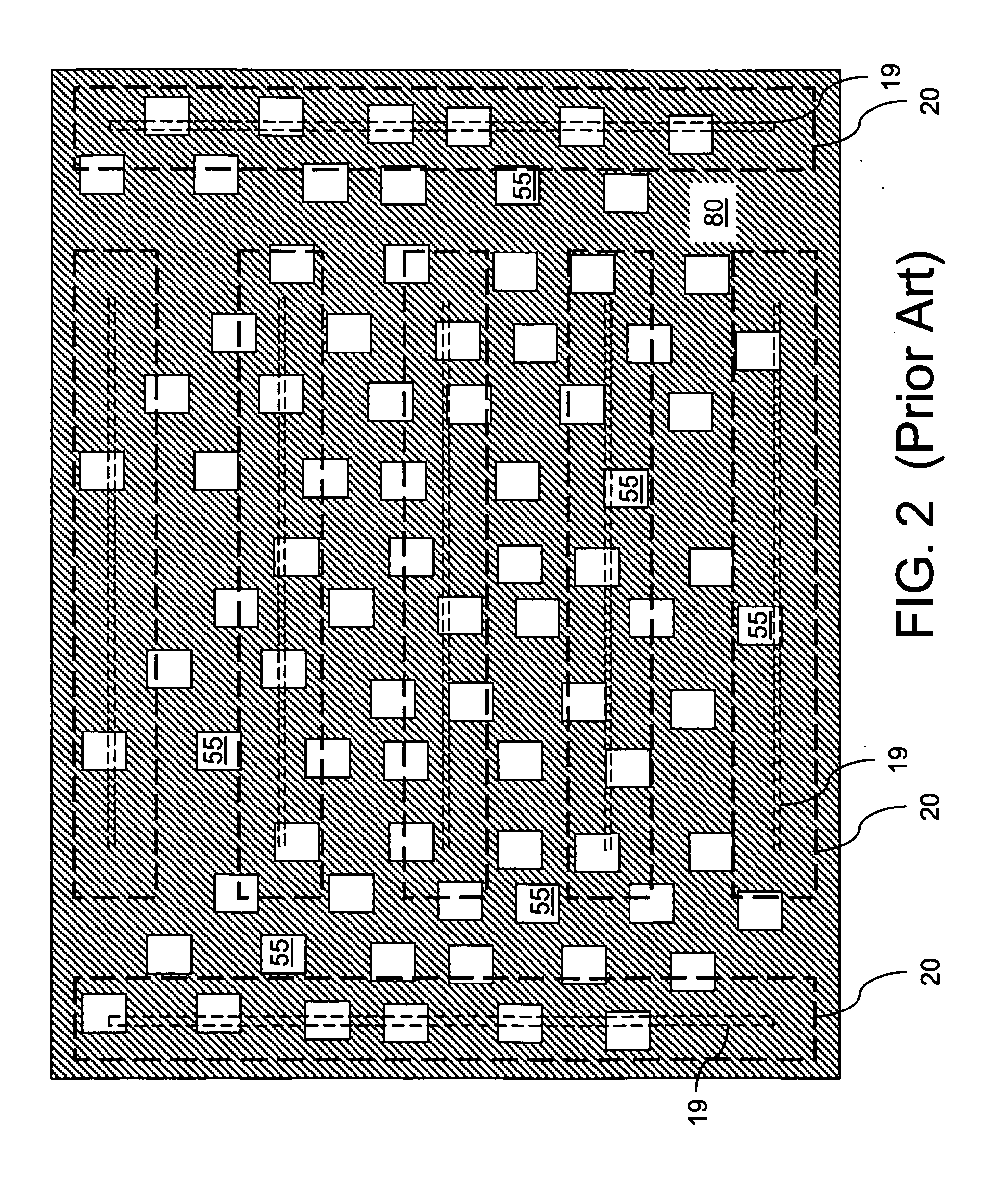
[0071]Referring to FIG. 5, a horizontal cross-sectional view of the exemplary semiconductor structure according to the present invention is shown along the plane X-X′ of FIG. 4. Locations of sidewalls of the TSVs 20 that abut the at least one line-level metal wiring structure 80 are shown in thick dotted lines as if a top-down see-through view was employed to illustrate the location of an array of cheesing holes relative to the sidewalls of the TSVs 20. The area of the seams 19 in the TSVs 20 are schematically represented by thin dotted lines as if a top-down see-through view was employed to illustrate the location of the array of cheesing holes relative to the seams 19.

[0072]The at least one line-level metal wiring structure 80 and the metal-wire-level dielectric layer 60 complimentarily fill the entirety of the a layer between top surfaces of the TSVs 20 and the top surfaces of the metal-wire-level dielectric layer 60. The entirety of the sidewalls of the at least one TSV 20 abuts...

second embodiment

[0077]Referring to FIG. 6, a horizontal cross-sectional view of the exemplary semiconductor structure according to the present invention is shown along the plane X-X′ of FIG. 4. Locations of sidewalls of the TSVs 20 that abut the at least one line-level metal wiring structure 80 are shown in thick dotted lines as if a top-down see-through view was employed to illustrate the location of an array of cheesing holes relative to the sidewalls of the TSVs 20. The area of the seams 19 in the TSVs 20 are schematically represented by thin dotted lines as if a top-down see-through view was employed to illustrate the location of the array of cheesing holes relative to the seams 19.

[0078]The at least one line-level metal wiring structure 80 and the metal-wire-level dielectric layer 60 complimentarily fill the entirety of the a layer between top surfaces of the TSVs 20 and the top surfaces of the metal-wire-level dielectric layer 60 in the same manner as in the first embodiment. The entirety of ...

third embodiment

[0082]Referring to FIG. 7, a horizontal cross-sectional view of the exemplary semiconductor structure according to the present invention is shown along the plane X-X′ of FIG. 4. Locations of sidewalls of the TSVs 20 that abut the at least one line-level metal wiring structure 80 are shown in thick dotted lines as if a top-down see-through view was employed to illustrate the location of an array of cheesing holes relative to the sidewalls of the TSVs 20. The area of the seams 19 in the TSVs 20 are schematically represented by thin dotted lines as if a top-down see-through view was employed to illustrate the location of the array of cheesing holes relative to the seams 19.

[0083]The at least one line-level metal wiring structure 80 and the metal-wire-level dielectric layer 60 complimentarily fill the entirety of the a layer between top surfaces of the TSVs 20 and the top surfaces of the metal-wire-level dielectric layer 60. The entirety of the sidewalls of the at least one TSV 20 abuts...


PUM


Abstract

An array of through substrate vias (TSVs) is formed through a semiconductor substrate and a contact-via-level dielectric layer thereupon. A metal-wire-level dielectric layer and a line-level metal wiring structure embedded therein are formed directly on the contact-via-level dielectric layer. The line-level metal wiring structure includes cheesing holes that are filled with isolated portions of the metal-wire-level dielectric layer. In one embodiment, the entirety of the cheesing holes is located outside the area of the array of the TSVs to maximize the contact area between the TSVs and the line-level metal wiring structure. In another embodiment, a set of cheesing holes overlying an entirety of seams in the array of TSVs is formed to prevent trapping of any plating solution in the seams of the TSVs during plating to prevent corrosion of the TSVs at the seams.

Description

FIELD OF THE INVENTION[0001]The present invention relates to semiconductor structures, and particularly to semiconductor structures including a line-level metal wiring structure and through substrate vias, methods of manufacturing the same, and design structures for the same.BACKGROUND OF THE INVENTION[0002]As continued semiconductor scaling faces difficulties at device dimensions approaching atomic scale, three-dimensional device integration offers a method of increasing semiconductor devices within a circuit. In three-dimensional integration, a plurality of semiconductor chips is vertically stacked to provide integration of semiconductor devices beyond a single semiconductor chip.[0003]One method of providing electrical connection between adjoining semiconductor chips is “flip chip” technology in which an array of solder balls are employed between two adjoined semiconductor chips that are vertically stacked face to face. However, flip chip technology provides electrical connection...

Claims


Application Information

Patent Timeline
Patent Type & Authority Applications(United States)
IPC IPC(8): H01L23/538H01L21/768G06F17/50
CPCH01L23/481H01L23/522H01L23/528H01L2924/0002H01L2924/00012H01L2924/00H01L23/14
Inventor COLLINS, DAVID S.JOSEPH, ALVINLINDGREN, PETER J.STAMPER, ANTHONY K.WATSON, KIMBALL M.
Owner GLOBALFOUNDRIES US INC
Why Eureka
Try Eureka