
Organic light emitting diode display

a light-emitting diode and organic technology, applied in the direction of discharge tube luminescnet screens, discharge tube/lamp details, electric discharge lamps, etc., can solve the problem of reducing the display characteristics of oled displays, and achieve the effect of suppressing the reflection of external light and improving visibility

Active Publication Date: 2010-02-11
SAMSUNG DISPLAY CO LTD
View PDF16 Cites 32 Cited by
  • Summary
  • Abstract
  • Description
  • Claims
  • Application Information

AI Technical Summary

Benefits of technology

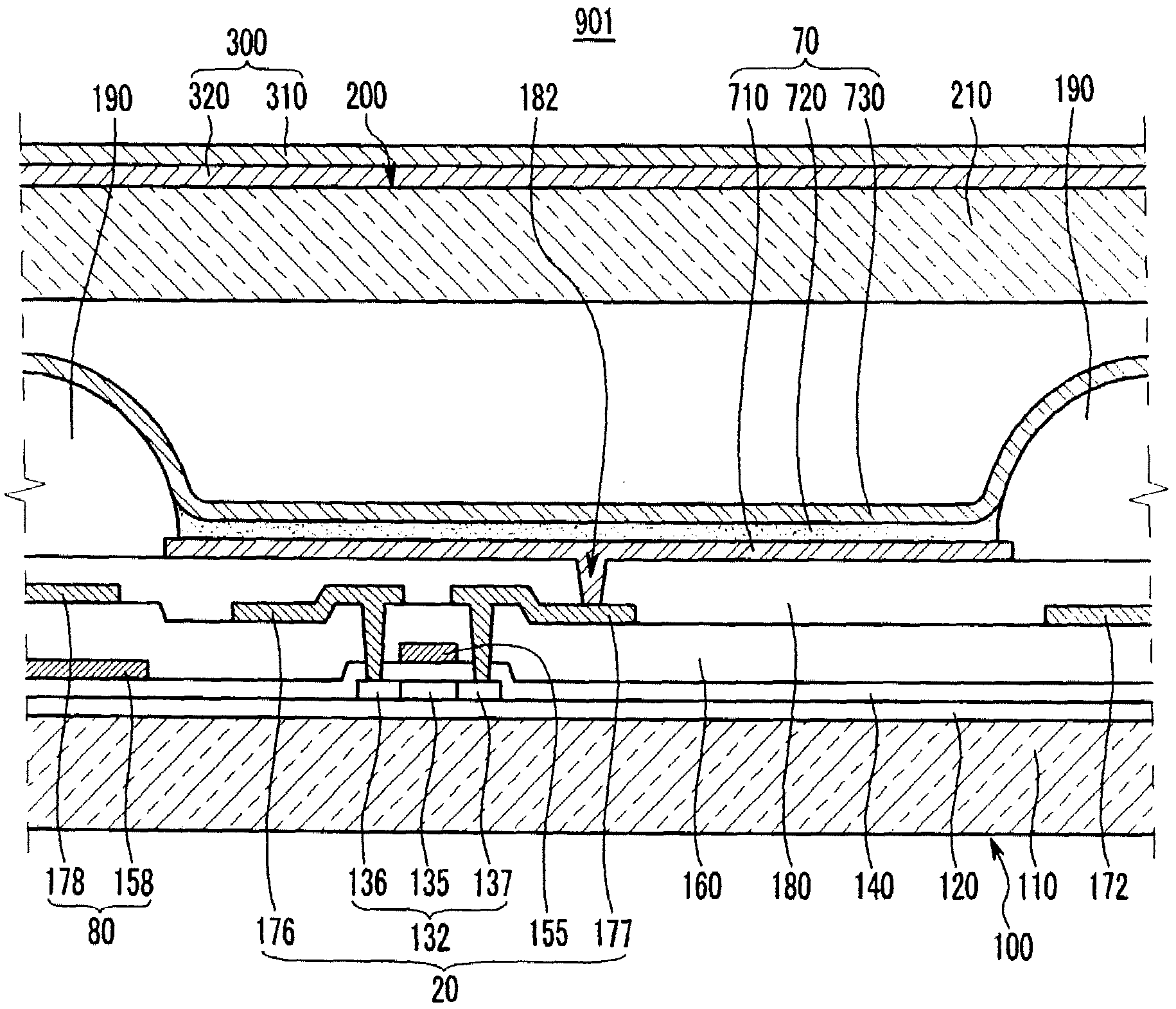
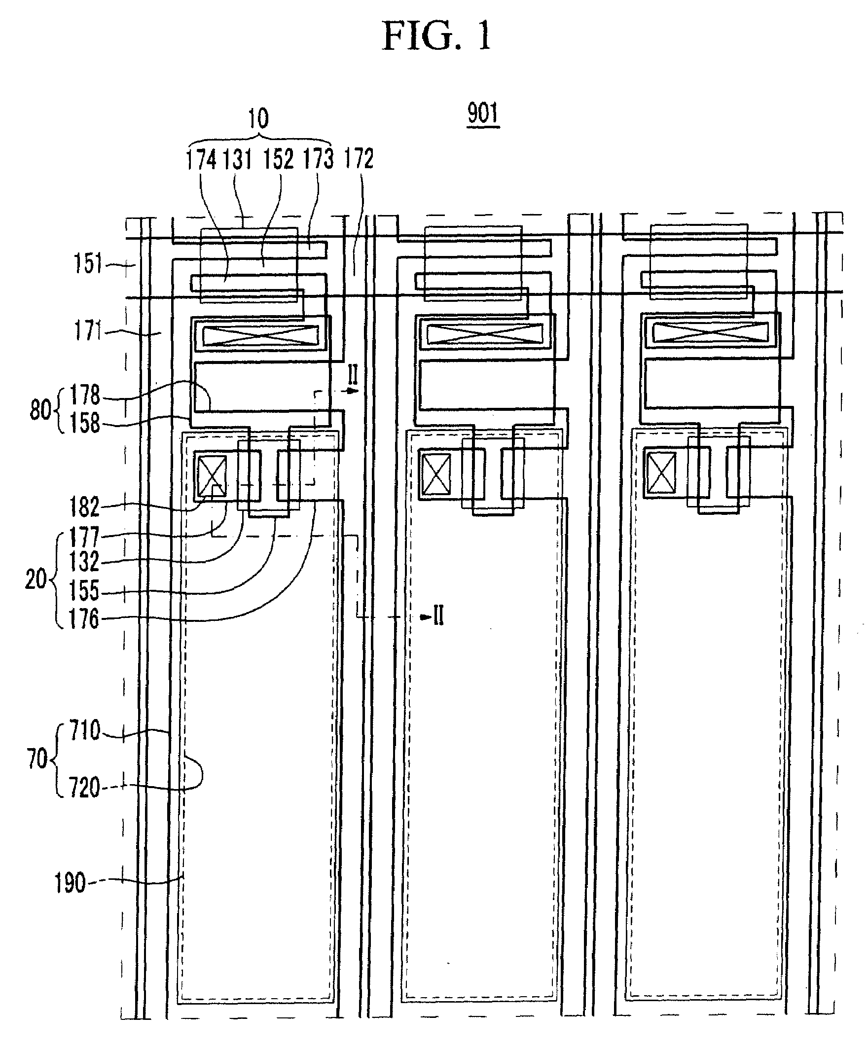
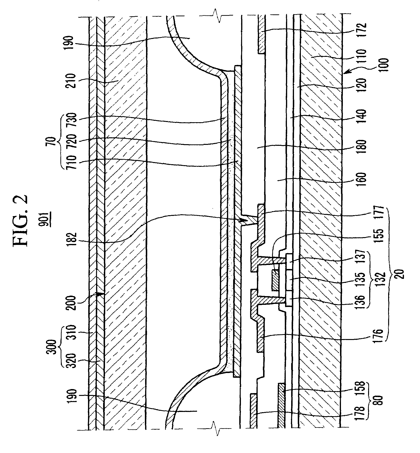
The present invention provides an OLED display that can improve visibility by suppressing the reflection of external light. This is achieved by using a polarizing member and a colored material on the OLED, which have different colors. The brightness of the mixture of the colors is lower than the brightness of each individual color. The polarizing member may include a polarization film and a ¼ wavelength phase delay film. The colored material may be the pixel defining layer or the sealing member. The TFT may include a conductive layer made of the same material as the polarizing member. The OLED display may further include a sealing member covering the TFT and OLED and a cover window on the sealing member. The colored material may be the cover window or the cover filling layer. The technical effect of this invention is to improve the visibility of OLED displays by reducing reflection of external light.

Problems solved by technology

The expression of black and the contrast of the OLED display deteriorate due to reflection of external light, thereby reducing the quality of the display characteristics of the OLED display.

Method used


Image

  • Organic light emitting diode display
  • Organic light emitting diode display
  • Organic light emitting diode display

Examples


Embodiment Construction

[0032]The present invention will be described more fully hereafter with reference to the accompanying drawings, in which exemplary embodiments of the invention are shown. As those skilled in the art would realize, the described embodiments may be modified in various different ways, all without departing from the spirit or scope of the present invention.

[0033]The drawings and description are to be regarded as illustrative in nature and not restrictive. In addition, the size and the thickness of each element in the drawing are random samples for better understanding and ease of description, and the present invention is not limited thereto. In the drawings, the thickness of layers, films, panels, regions, etc., are exaggerated for clarity. It will be understood that when an element such as a layer, film, region, or substrate is referred to as being “on” another element, it can be directly on the other element or intervening elements may also be present. In contrast, when an element is ...


PUM


Abstract

An organic light emitting diode (OLED) display including a substrate, a thin film transistor (TFT) formed on the substrate, an OLED, a colored polarizing member on the OLED, and a colored material on the OLED and having a color that is different from that of the polarizing member. The OLED includes a pixel electrode, an organic emission layer on the pixel electrode, and a common electrode on the organic emission layer, wherein the pixel electrode is coupled to the TFT.

Description

CROSS-REFERENCE TO RELATED APPLICATIONS[0001]This application claims priority to and the benefit of Korean Patent Application Nos. 10-2008-0076440 and 10-2009-0001161 filed in the Korean Intellectual Property Office on Aug. 5, 2008 and Jan. 7, 2009, respectively, the entire contents of which are incorporated herein by reference.BACKGROUND OF THE INVENTION[0002]1. Field of the Invention[0003]The present invention relates to an organic light emitting diode (OLED) display.[0004]2. Description of the Related Art[0005]An OLED display includes a plurality of OLEDs having a hole injection electrode, an organic emission layer, and an electron injection electrode. Light is emitted by energy generated when excitons, that is, electron-hole pairs, are combined to drop from an excited state to a ground state, and the OLED display displays an image utilizing the emitted light.[0006]Accordingly, the OLED display has self-luminance characteristics, and compared to a liquid crystal display (LCD), th...

Claims


Application Information

Patent Timeline
Patent Type & Authority Applications(United States)
IPC IPC(8): H01L27/32
CPCH01L27/3244H01L51/5281H10K59/12H10K59/8791H10K50/86
Inventor KIM, EUN-AHJUNG, WOO-SUKJEONG, HEE-SEONGPARK, SOON-RYONGLEE, JOO-HWAKWAK, NOH-MINJEONG, CHUL-WOOJEON, HEE-CHUL
Owner SAMSUNG DISPLAY CO LTD
Learn More