Operational amplifier circuit and display panel driving apparatus
- Summary
- Abstract
- Description
- Claims
- Application Information
AI Technical Summary
Benefits of technology
Problems solved by technology
Method used
Image

Examples
first embodiment
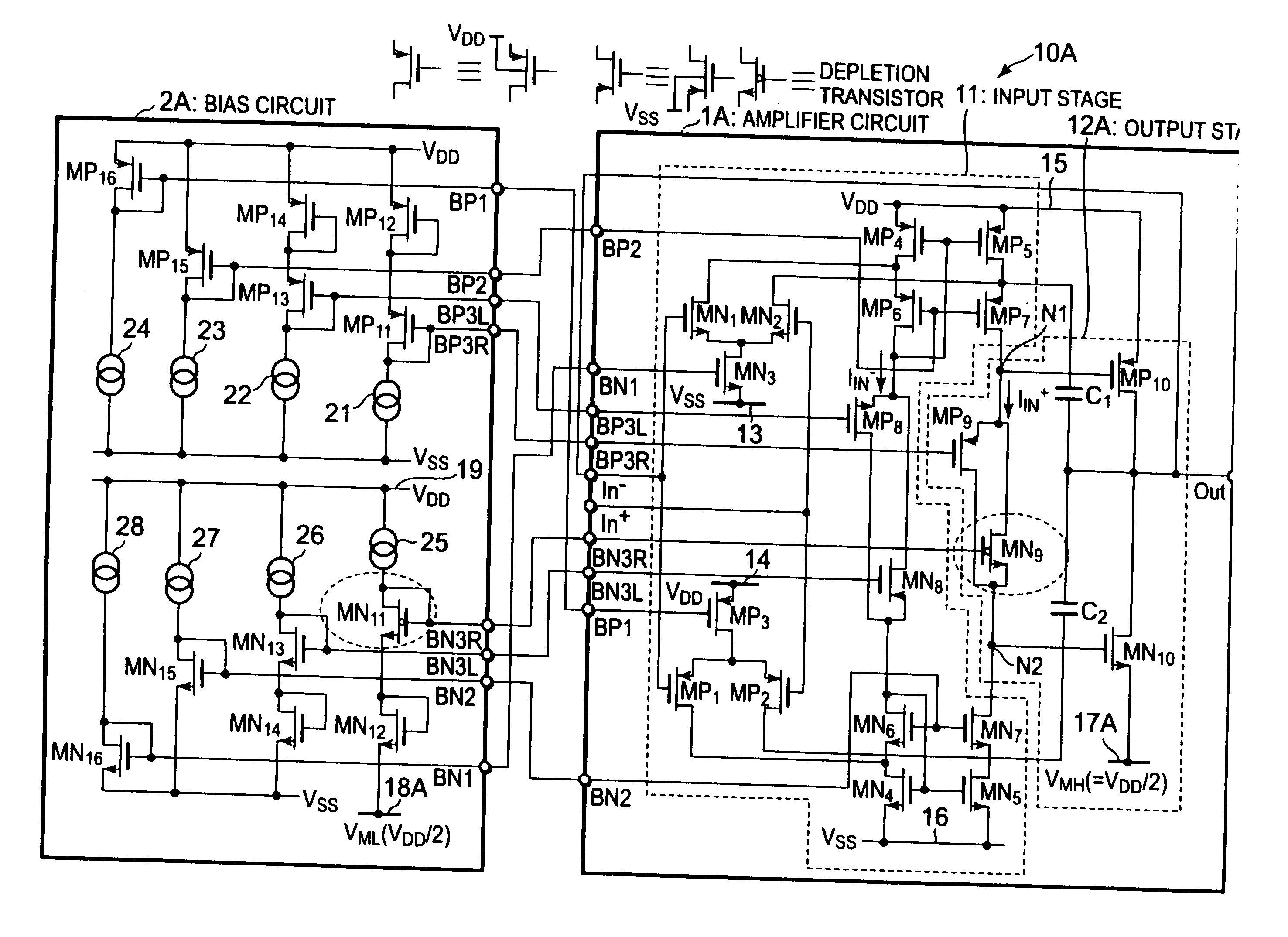
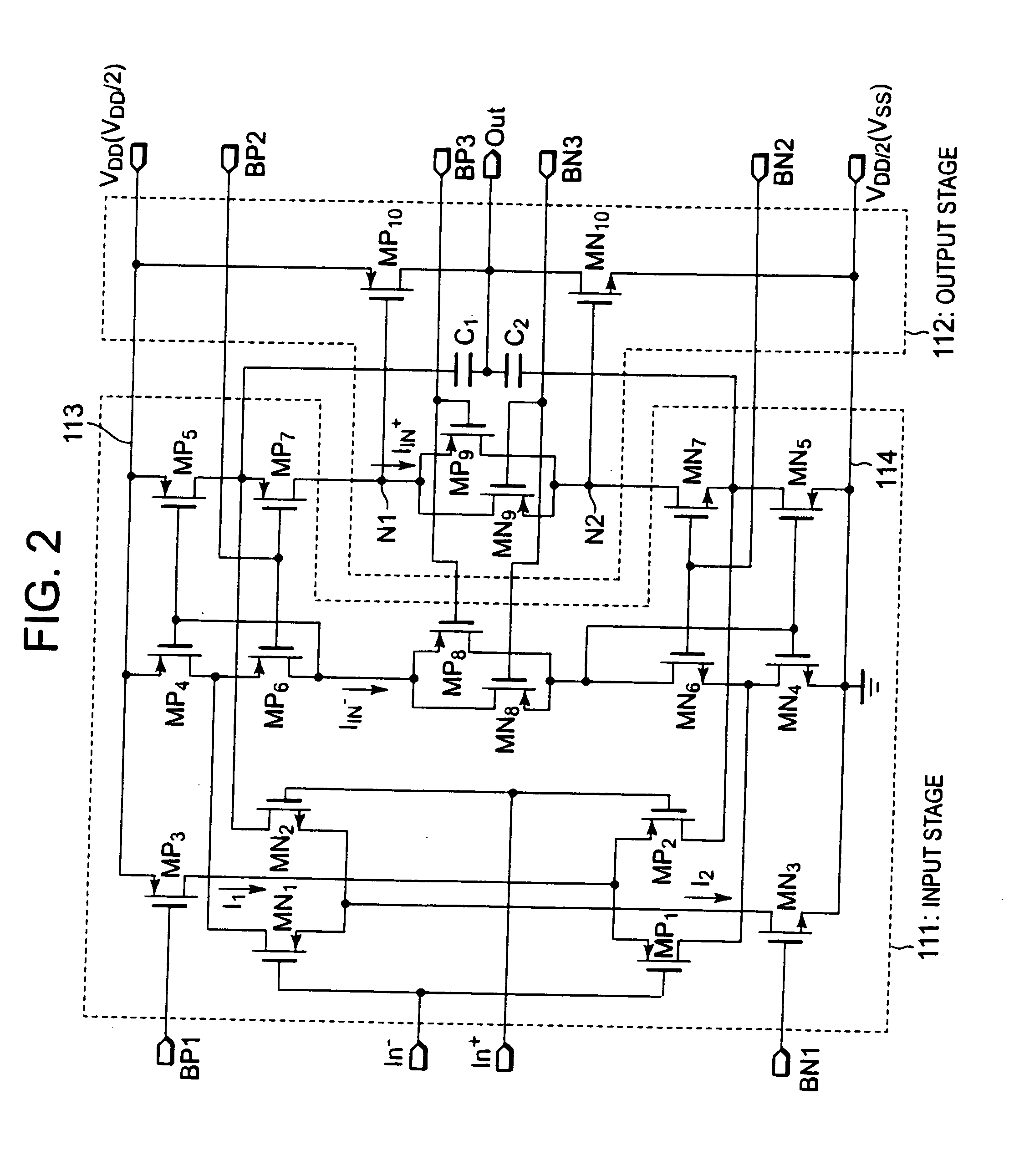
[0034]FIG. 3 is a circuit diagram showing the configuration of an operational amplifier circuit 10A according to a first embodiment of the present invention. The operational amplifier circuit 10A according to the first embodiment includes an amplifier circuit 1A and a bias circuit 2A for supplying a bias voltage to the amplifier circuit 1A. The amplifier circuit 1A includes an input stage 11 and an output stage 12A.
[0035]The input stage 11 is a circuit part for generating an internal current IIn+ corresponding to a potential difference between an inverting input terminal In− and a non-inverting input terminal In+, and for supplying the internal current IIn+ to the output stage. The input stage 11 includes PMOS transistors MP1 to MP8 and NMOS transistors MN1 to MN8.
[0036]The gates of the NMOS transistors MN1, MN2 are connected to the inverting input terminal In− and the non-inverting input terminal In+, respectively. The sources of the NMOS transistors MN1, MN2 are commonly connected...
second embodiment
[0078]FIG. 6 is a circuit diagram showing the configuration of an operational amplifier circuit 10B according to a second embodiment of the present invention. The operational amplifier circuit 10B shown in FIG. 6 has the configuration which is similar to that of the operational amplifier circuit 10A shown in FIG. 3. The differences therebetween are the following four points. First, in the operational amplifier circuit 10B shown in FIG. 6, an output stage 12B of an amplifier circuit 1B operates by receiving the ground voltage VSS and an intermediate power supply voltage VML which is lower than the power supply voltage VDD. Specifically, the source of the PMOS transistor MP10 is connected to a power supply line 17B through which the intermediate power supply voltage VML is supplied, and the source of the NMOS transistor MN10 is connected to the ground line 16 through which the ground voltage VSS is supplied. Here, the intermediate power supply voltage VML is a voltage which is lower t...
third embodiment
[0095]FIG. 8 is a circuit diagram showing the configuration of an operational amplifier circuit 10C according to a third embodiment of the present invention. The configuration of the operational amplifier circuit 10C shown in FIG. 8 is similar to that of the operational amplifier circuit 10A shown in FIG. 3, and the two operational amplifier circuits are different from each other in terms of the following points.
[0096]First, the operational amplifier circuit 10C shown in FIG. 8 does not use the intermediate power supply voltage which is higher than the ground voltage VSS and lower than the power supply voltage VDD. In other words, an output stage 12C of an amplifier circuit 1C operates by receiving the power supply voltage VDD and the ground voltage VSS. Specifically, the source of the PMOS transistor MP10 is connected to the power supply line 15 through which the power supply voltage VDD is supplied, whereas the source of the NMOS transistor MN10 is connected to the ground line 16 ...
PUM
 Abstract
Description
Claims
Application Information
 - Generate Ideas
- Intellectual Property
- Life Sciences
- Materials
- Tech Scout
- Unparalleled Data Quality
- Higher Quality Content
- 60% Fewer Hallucinations
Browse by: Latest US Patents, China's latest patents, Technical Efficacy Thesaurus, Application Domain, Technology Topic, Popular Technical Reports.
© 2025 PatSnap. All rights reserved.Legal|Privacy policy|Modern Slavery Act Transparency Statement|Sitemap|About US| Contact US: help@patsnap.com