
Pick-up apparatus for semiconductor chips and pick-up method for semiconductor chips using the same

a technology of pick-up apparatus and semiconductor chip, which is applied in the direction of layered products, chemistry apparatus and processes, door/window protective devices, etc., can solve the problems of increasing the inability of semiconductor chips to resist, and the increase of the problem of cracking or chipping of semiconductor chips, so as to prevent cracking, increase fabrication efficiency, and remove even thin semiconductor chips

Inactive Publication Date: 2010-02-18
RENESAS ELECTRONICS CORP
View PDF7 Cites 8 Cited by
  • Summary
  • Abstract
  • Description
  • Claims
  • Application Information

AI Technical Summary

Benefits of technology

[0011]According to the present invention, the slit provided on a side where the slider comes into contact with the adhesive sheet is in communication with the slider housing portion. As a result of this, the suction mechanism suctions the slit by suctioning the slider housing portion and can generate a negative pressure in a space formed by the slit and the adhesive sheet. Thanks to this negative pressure it is possible to suction the adhesive sheet and it is possible to peel off part of the adhesive sheet from the semiconductor chip. Because a negative pressure is generated also in a space formed by a peripheral edge part of the slider housing portion and the adhesive sheet, it is also possible to suction the adhesive sheet opposed to the peripheral edge part of the slider housing portion to peel it from the semiconductor chip. Therefore, a plurality of initiation points of delamination which are distributed from each other are formed and when the slider is moved horizontally with respect to the semiconductor chip, it is possible to increase the size of delaminated areas gradually from the above-described initiation points. Hence, it is possible to distribute the force acting on the semiconductor chip during the delamination of the adhesive sheet from the semiconductor chip and as a result of this, it is possible to prevent cracking even in the case of a large thin chip.
[0014]According to the present invention, it is possible to peel off even a thin semiconductor chip from an adhesive sheet while preventing cracking. Therefore, it is possible to increase the fabrication efficiency in the pick-up step of semiconductor chips.

Problems solved by technology

However, in the related arts described in Japanese Patent Laid-Open No. 2003-224088 and Japanese Patent Laid-Open No. 2005-328054, when attempting to pick up a thin semiconductor chip, the semiconductor chip cannot withstand the force which peels the chip from the adhesive sheet and the semiconductor chip will become cracked or chipped.
The larger the semiconductor chip, the greater this problem will be.
Therefore, the yield of large thin semiconductor chips may decrease.

Method used


Image

  • Pick-up apparatus for semiconductor chips and pick-up method for semiconductor chips using the same
  • Pick-up apparatus for semiconductor chips and pick-up method for semiconductor chips using the same
  • Pick-up apparatus for semiconductor chips and pick-up method for semiconductor chips using the same

Examples


first embodiment

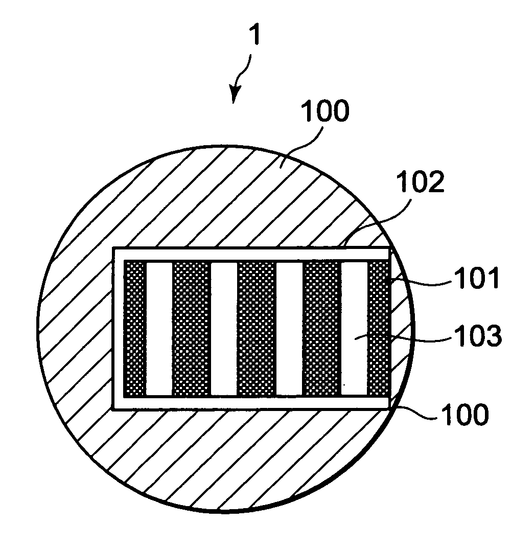
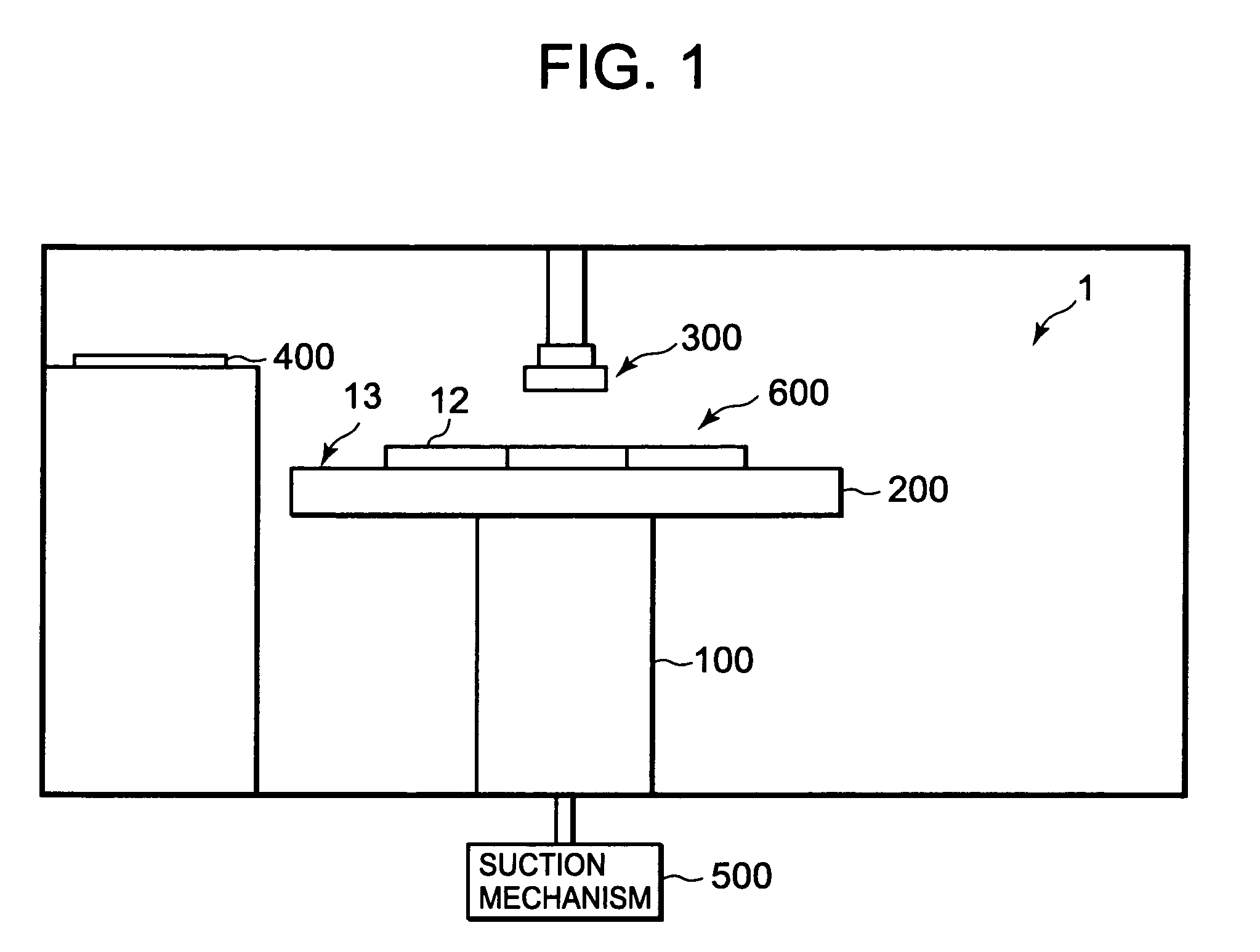
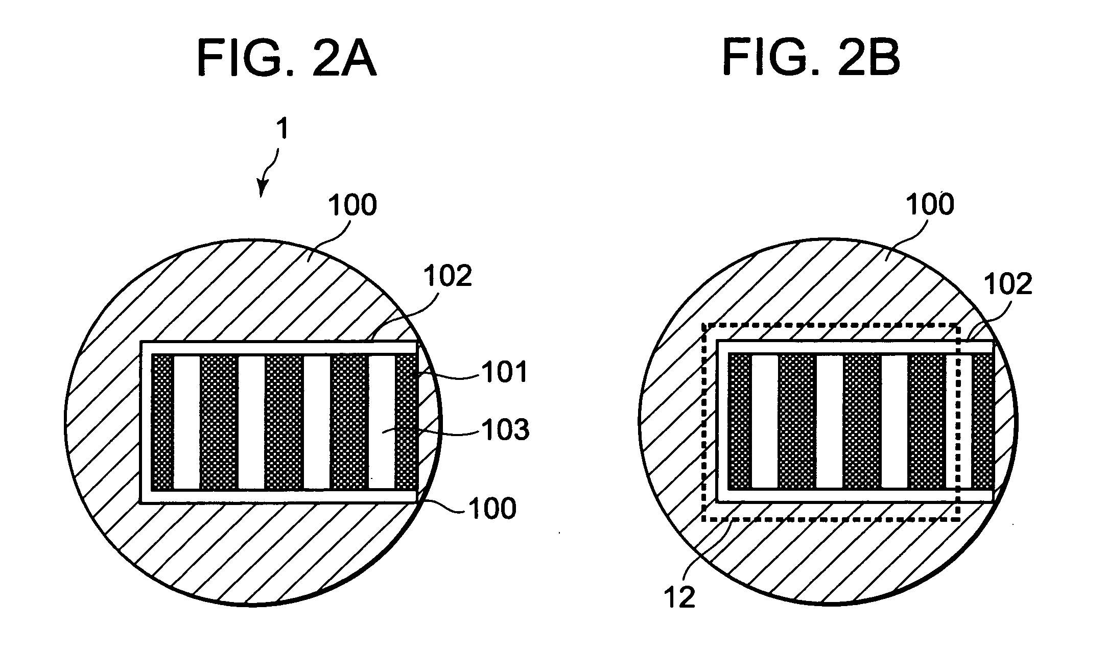
[0021]FIG. 1 and FIGS. 2A and 2B are schematic diagrams showing a pick-up apparatus 1 of the first embodiment. FIG. 1 is a side view of the pick-up apparatus 1 of the first embodiment. FIGS. 2A and 2B are plan views of the pick-up apparatus 1 of the first embodiment.

[0022]As shown in FIG. 1, the pick-up apparatus 1 is a pick-up apparatus for semiconductor chips which delaminates a semiconductor chip 12 mounted on one surface (a front surface) of a dicing sheet (an adhesive sheet) 13 from the dicing sheet 13. The pick-up apparatus 1 has a stage 100 on which a dicing sheet 13 is placed, a slider 101 which comes into contact with the other surface (a back surface) of the dicing sheet 13 and moves horizontally, in plan view, with respect to a semiconductor chip 12, a slider housing portion 102 which is formed in the stage 100 and houses the slider 101, and a suction mechanism 500 which is coupled to the stage 100 and suctions the slider housing portion 102. On the stage 100, the dicing ...

second embodiment

[0035]FIGS. 4A to 4C and FIGS. 5A and 5B are plan views showing a pick-up apparatus 2 of the second embodiment. FIGS. 4A to 4C and FIG. 5B are plan views of a stage 100 of the pick-up apparatus 2. FIG. 5A is an enlarged view of part of a slider housing portion 102. In FIGS. 5A and 5B, a slit 103 is omitted. The pick-up apparatus 2 differs from the pick-up apparatus 1 in that, for each semiconductor chip 12, a plurality of sliders 201a, 201b, 201c, 201d are formed be parallel in a manner spaced from each other and in that each of the sliders is movable individually horizontally, in plan view, with respect to a semiconductor chip 12. The sectional view of the pick-up apparatus 2 is the same as in FIGS. 3A to 3C.

[0036]Although it is possible to set, as the spacing between the sliders, an optimum distance to match the size and thickness of a chip, the magnitude of a negative pressure generated from a suction mechanism 500, and the adhesive force of a dicing sheet 13, it is possible to s...


PUM


Abstract

Even in the case of a thin semiconductor chip, the semiconductor chip is delaminated from an adhesive sheet so as to prevent cracking. A pick-up apparatus 1 has a stage 100 on which a dicing sheet 13 is placed, a slider which comes into contact with a back surface of the dicing sheet 13 and moves horizontally, in plan view, with respect to a semiconductor chip 12, a slider housing portion which is formed in the stage 100 and houses the slider, and a suction mechanism 500 which is coupled to the stage 100 and suctions the slider housing portion. On the stage 100, the dicing sheet 13 is placed in a position where the semiconductor chip 12 is opposed to the slider housing portion. The slider is provided with a plurality of slits on a side where the slider comes into contact with the dicing sheet 13. The slit is in communication with the slider housing portion 102.

Description

BACKGROUND OF THE INVENTION[0001]1. Field of the Invention[0002]The present invention relates to a pick-up apparatus for semiconductor chips which delaminates a semiconductor chip mounted on a surface of an adhesive sheet from the adhesive sheet and a pick-up method for semiconductor chips using this pick-up apparatus.[0003]2. Description of the Related Art[0004]Conventional pick-up apparatus used in the manufacturing process of semiconductor devices are described in Japanese Patent Laid-Open No. 2003-224088 and Japanese Patent Laid-Open No. 2005-328054, for example.[0005]The pick-up apparatus for semiconductor chips described in Japanese Patent Laid-Open No. 2003-224088 is such that a dicing sheet to which a semiconductor chip (hereinafter also called a chip) is stuck is placed on a stage, a roller having a plurality of protruding members is rotated, and these protruding members are pushed up from under the dicing sheet during the rotation of the roller.[0006]The pick-up apparatus ...

Claims


Application Information

Patent Timeline
IPC IPC(8): B32B38/00
CPCH01L21/67132Y10T156/1132Y10T156/1944H01L21/6838
Inventor KOIKE, DAISUKE
Owner RENESAS ELECTRONICS CORP
Learn More