Power noise detecting device and power noise control device using the same

a power noise and detection device technology, applied in the field of semiconductor devices, can solve the problems of power noise not being reduced to the desired level, components having a negative influence on the proper operation of the semiconductor ic device, noise generated in the supplied power, etc., and achieve the effect of accurately detecting power noise and minimizing power nois

Inactive Publication Date: 2010-02-18
SK HYNIX INC
View PDF31 Cites 22 Cited by
  • Summary
  • Abstract
  • Description
  • Claims
  • Application Information

AI Technical Summary

Benefits of technology

[0008]A power noise detecting device and a power noise control device using the same capable of accurately detecting power noise and minimizing the power noise by implementing a simple circuit are described herein.

Problems solved by technology

Accordingly, the parasitic components may have an negative influence on the proper operation of the semiconductor IC device.
For example, the parasitic components may cause noise to be generated in the supplied power.
However, since the semiconductor IC is commonly designed only to minimize the ESR, there is a problem in that the power noise cannot be reduced to a desired level.

Method used


Image

  • Power noise detecting device and power noise control device using the same
  • Power noise detecting device and power noise control device using the same
  • Power noise detecting device and power noise control device using the same

Examples


Embodiment Construction

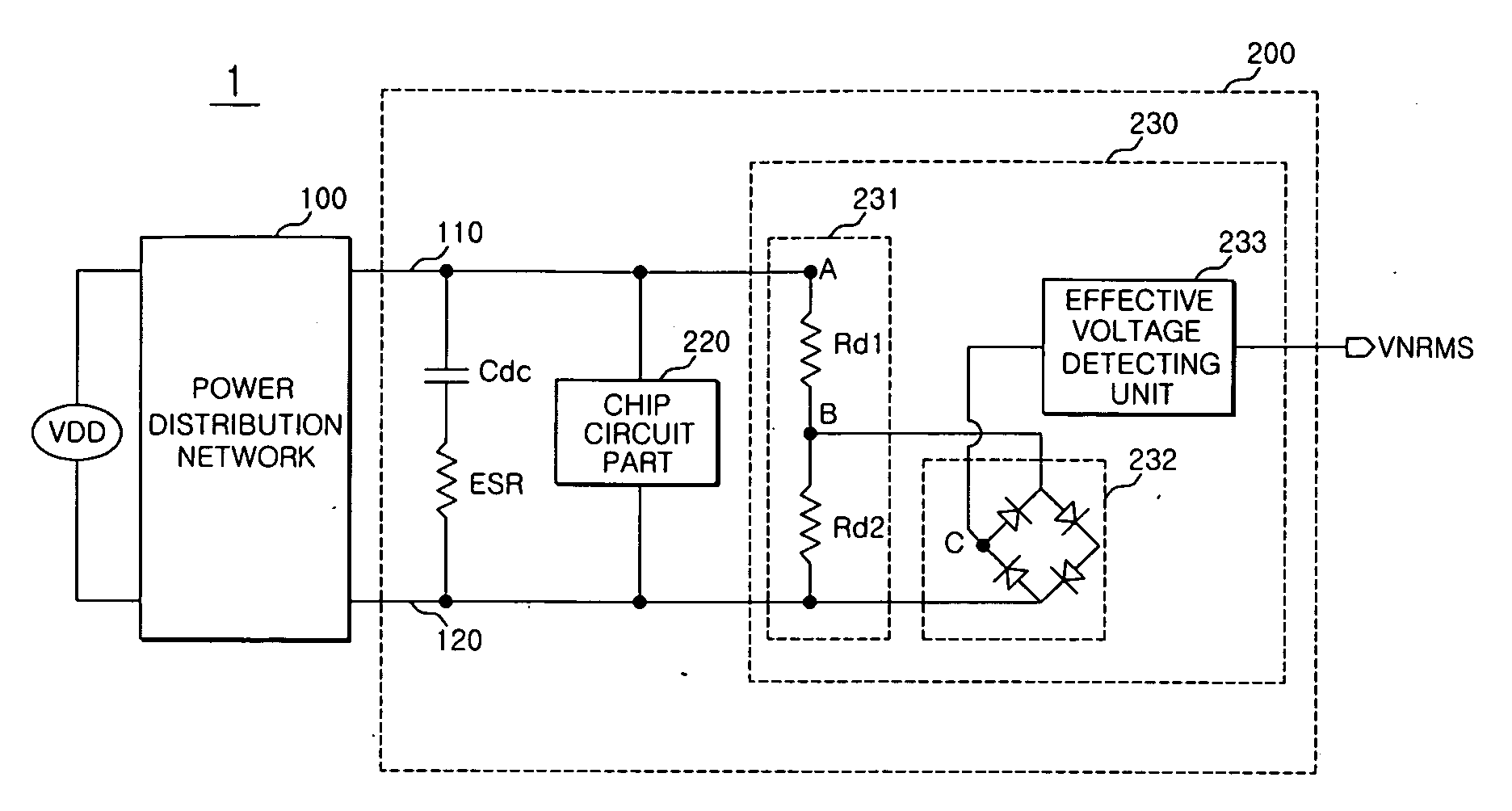
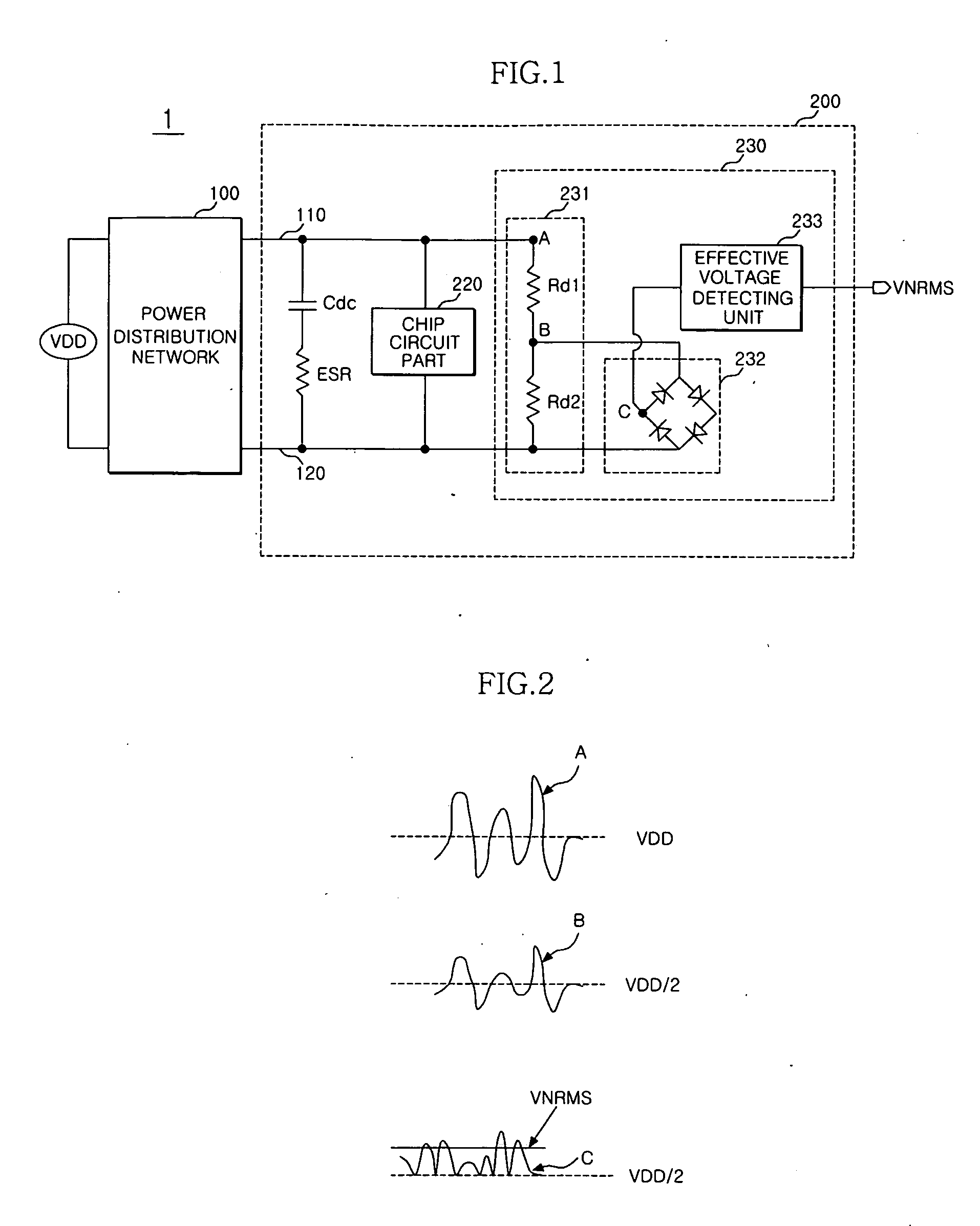
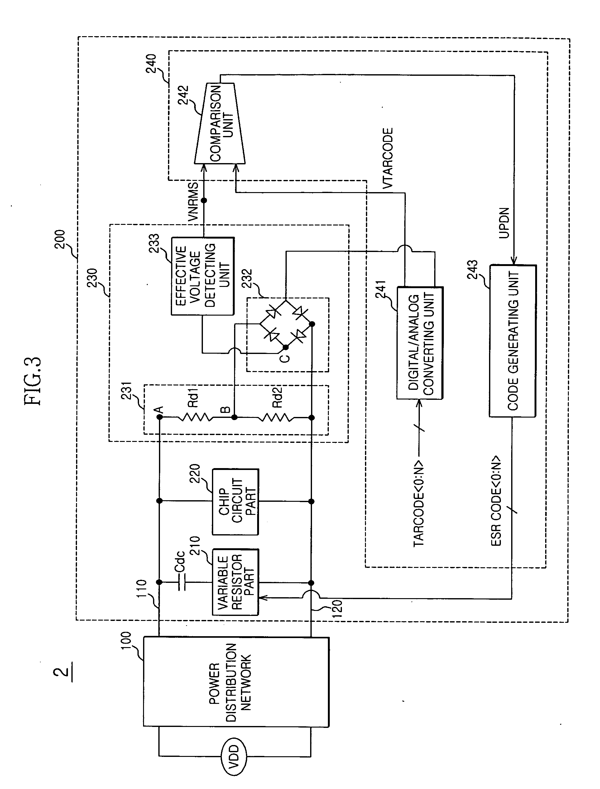
[0017]FIG. 1 is a schematic circuit diagram of an exemplary power noise detecting device according to one embodiment. In FIG. 1, a power noise detecting device 1 can be configured to include power lines 110 and 120 via a chip circuit part 220, and a power noise detecting part 230 for detecting the noise of power applied through the power lines 110 and 120, which can be installed in / on a semiconductor chip, such as a semiconductor IC 200.

[0018]A power distribution network 100 can be connected to the semiconductor IC 200 via the power lines 110 and 120. In addition, a decoupling capacitor Cdc, a parasitic resistance component, i.e., an Equivalent Series Resistance (ESR) generated by the decoupling capacitor Cdc, and the chip circuit part 220 can be interconnected between the power lines 110 and 120.

[0019]The chip circuit part 220 can represent a portion or an entirety of a circuit configuration including various signal processing circuits, memory cells, and the like constituting the s...


PUM


Abstract

A power noise detecting device includes a plurality of power lines, and a power noise detecting part configured to detect power noise by rectifying voltages of the plurality of power lines and converting the rectified voltages into effective voltages.

Description

CROSS-REFERENCES TO RELATED APPLICATION[0001]The present application claims priority under 35 U.S.C. § 119(a) to Korean application number 10-2008-0078808, filed on Aug. 12, 2008, filed in the Korean Intellectual Property Office, which is incorporated herein by reference in its entirety as set forth in full.BACKGROUND[0002]1. Technical Field[0003]The embodiments described herein relate to a semiconductor device, and more particularly, to a power noise detecting device and a power noise control device using the same.[0004]2. Related Art[0005]A power distribution network (PDN) is configured between a semiconductor integrated circuit (IC) device and an external apparatus to supply power to the semiconductor IC device from the external apparatus through the power distribution network. Parasitic components, such as capacitances, inductances, resistances, and the like, exist on the power distribution network. Accordingly, the parasitic components may have an negative influence on the prop...

Claims


Application Information

Patent Timeline
Patent Type & Authority Applications(United States)
IPC IPC(8): G01R19/22
CPCH03K19/00346H03H1/0007
Inventor KIM, HYUNG-SOOKIM, YONG-JUHAN, SUNG-WOOSONG, HEE-WOONGOH, IC-SUHWANG, TAE-JINCHOI, HAE-RANGLEE, JI-WANGJANG, JAE-MINPARK, CHANG-KUN
Owner SK HYNIX INC
Why Eureka
Try Eureka