Image exposing method and apparatus

a technology of image exposing and exposing surface, which is applied in the direction of photomechanical equipment, instruments, printing, etc., can solve the problems of small amount of light incident on the exposing surface, degraded image sharpness, and large pixel size in the projected image, and achieve high resolution images and reduce the resolution of exposed images

Inactive Publication Date: 2010-02-25
FUJIFILM CORP
View PDF3 Cites 8 Cited by
  • Summary
  • Abstract
  • Description
  • Claims
  • Application Information

AI Technical Summary

Benefits of technology

[0025]In the image exposing apparatuses according to the present invention, the pixel images of the pixel sections of the spatial optical modulation device are focused at the respective aperture planes of the aperture array, which are then focused by the microlens array. This arrangement allows the image location focused by the microlens array to be maintained unchanged for the light from the pixel sections of the spatial optical modulation device entering the respective aperture planes at any incident angle. In the first image exposing apparatus in which the image focused by the microlens array is projected on the photosensitive material using a further optical system or in the second image exposing apparatus in which the image focused by the microlens array is directly focused on the photosensitive material, degradation in the resolution of the exposed image due to fluctuations in the beam positions on the photosensitive material arising from changes in the incident angle described above may be prevented.
[0026]Further, pixel images positioned at respective aperture planes of the aperture array are focused by the microlens array as described above, so that the beam diameter on the photosensitive material remains unchanged even when the beam diameter of the beam entering the aperture array 59 is fluctuated due to field curvature, astigmatic difference, and the like of the image focusing optical system disposed in front of the aperture array. This also allows a high resolution image to be exposed.
[0027]Preferably, the image exposing apparatuses according to the present invention are constructed to employ a DMD that includes microlenses disposed two-dimensionally as the spatial optical modulation device, since aforementioned problems which are more likely to occur in the DMD due to the transient response characteristic of the micromirrors may be prevented.
[0028]The image exposing method according to the present invention is a method for exposing a predetermined pattern on a photosensitive material using any of the image exposing apparatuses of the present invention. Therefore, the method may prevent the aforementioned problems reliably.

Problems solved by technology

Thus, the pixel size in the projected image becomes larger and the sharpness of the image is degraded.
Further, a small amount of light may sometimes be incident on the exposing surface even when the pixels (micromirrors) of the DMD are turned off to shut out the light.
The conventional image exposing system that combines a spatial optical modulation device with a microlens array has a problem that the light beam focused by each microlens of the microlens array fluctuates to a small extent on the photosensitive material.
This results in as if the exposure was performed by a light beam having a larger spot diameter and the resolution of the exposed image is degraded.
In particular, this problem is more significant when a DMD is used as the spatial optical modulation device.
This leads to positional fluctuations of the light beam on the photosensitive material.
So far the problem when a DMD is used as the spatial optical modulation device has been described.
Even in the case where a different type of spatial optical modulation device is employed, if the beam angle of the light entering the microlens fluctuates for one reason or another, the same problem of degradation in the resolution of the exposed image occurs.

Method used


Image

  • Image exposing method and apparatus
  • Image exposing method and apparatus
  • Image exposing method and apparatus

Examples


Embodiment Construction

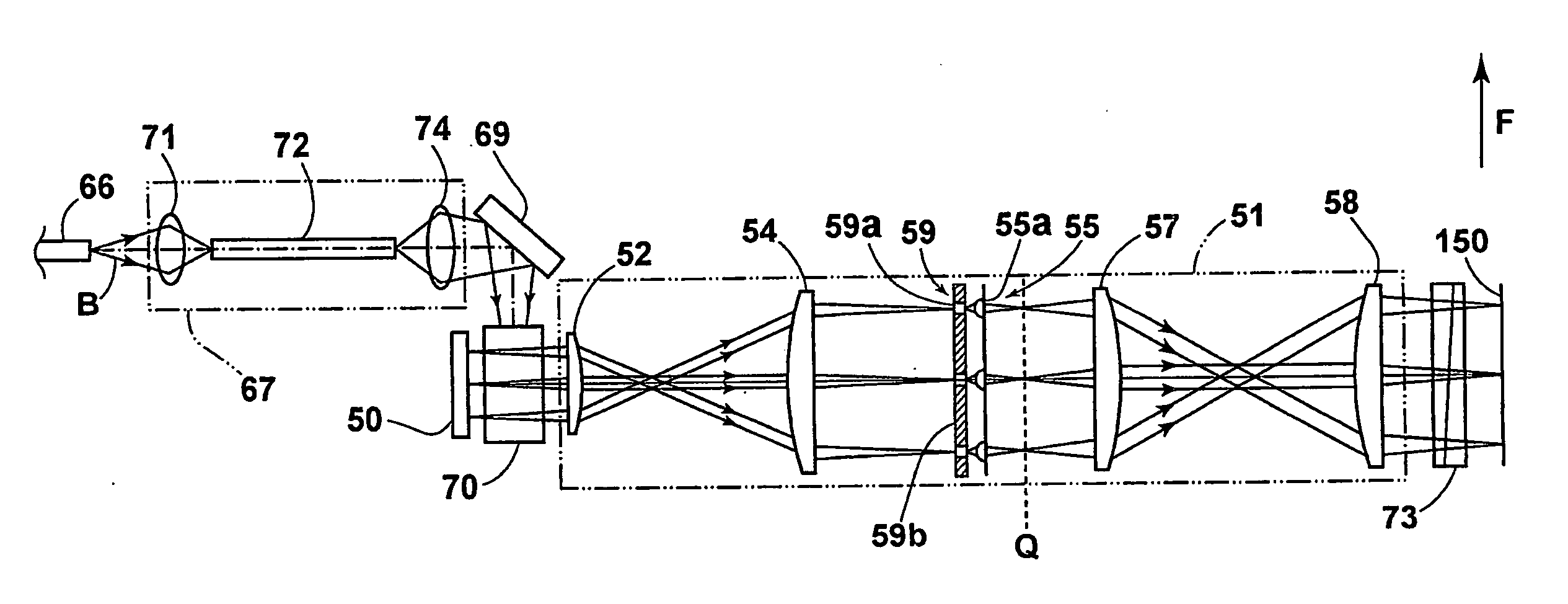
[0052]Hereinafter, preferred embodiments of the present invention will be described in detail with reference to the accompanying drawings. The image exposing apparatus according to a first embodiment will be described first.

[Construction of the Image Exposing Apparatus]

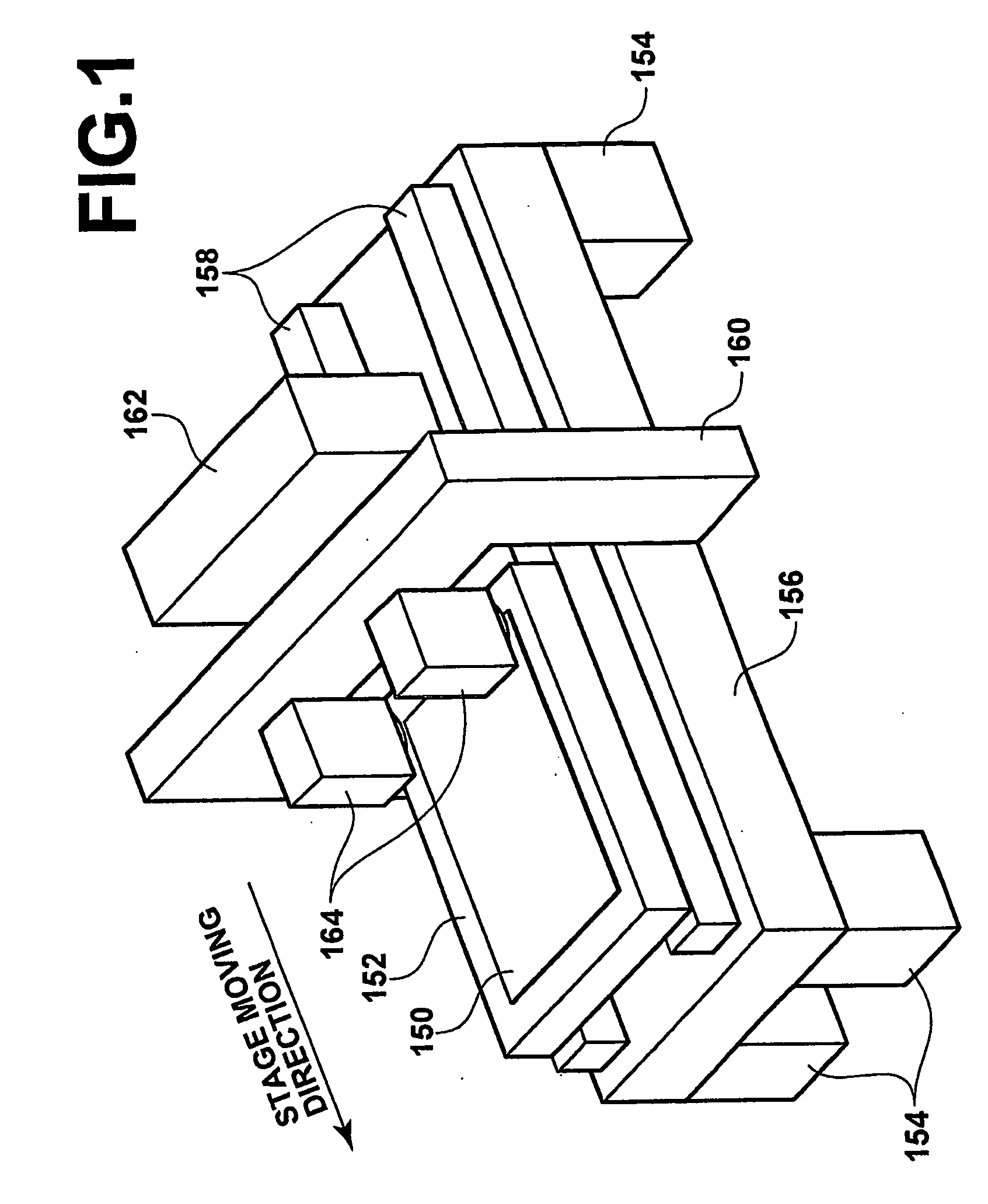
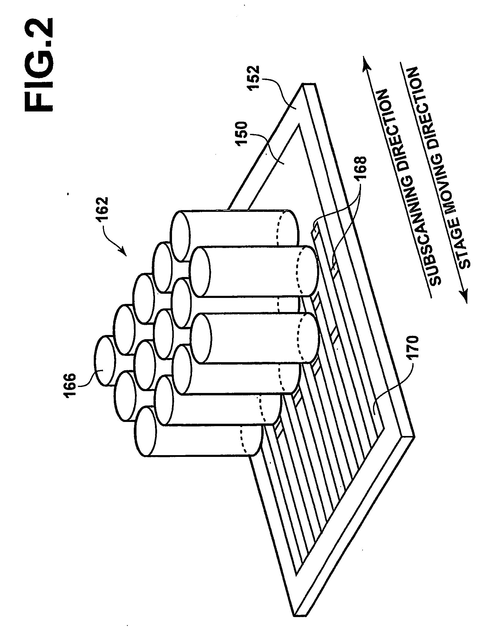
[0053]As shown in FIG. 1, the image exposing apparatus of the present embodiment includes a plate-like moving stage 150 for holding a sheet-like photosensitive material 12 thereon by suction. Two guides 158 extending along the moving direction of the stage are provided on the upper surface of a thick plate-like mounting platform 156 which is supported by four legs 154. The stage 152 is arranged such that its longitudinal direction is oriented to the moving direction of the stage, and movably supported by the guides 158 to allow back-and-forth movements. The image exposing apparatus of the present embodiment further includes a stage driving unit 304 (FIG. 15), which will be described later, for driving the stage 152 th...


PUM


Abstract

An image exposing apparatus capable of avoiding degradation in the resolution of an exposed image due to fluctuations in the traveling direction of light that focuses pixel images of the pixel sections of a spatial optical modulation device. The apparatus includes the spatial optical modulation device, such as a DMD having multitudes of pixel sections disposed two-dimensionally; a light source; and image focusing optical systems. It further includes an aperture array disposed at the image location focused by the image focusing optical systems such that each of the pixel images of the pixel sections is positioned at the plane of each of the apertures. The pixel images positioned at the aperture planes of the aperture array are focused into an image by a microlens array, which is then projected onto a photosensitive material by optical systems.

Description

TECHNICAL FIELD[0001]The present invention relates to an image exposing apparatus. More specifically, the present invention is directed to an image exposing apparatus, in which a photosensitive material is exposed by focusing thereon an optical image represented by light modulated by a spatial optical modulation device.[0002]The present invention also relates to an image exposing method that uses such an image exposing apparatus.BACKGROUND ART[0003]Image exposing systems, in which light modulated by a spatial optical modulation device is passed through an image focusing optical system to focus an image represented by the light on a predetermined photosensitive material in order to expose it with the image are known. Basically, such an image exposing system includes a spatial optical modulation device having multitudes of pixel sections arranged two-dimensionally, each for modulating irradiated light in accordance with a control signal; a light source for irradiating light on the spa...

Claims


Application Information

Patent Timeline
Patent Type & Authority Applications(United States)
IPC IPC(8): G21K5/10
CPCG03B27/32G03F7/70291G03F7/70275G03F7/7025
Inventor ISHIKAWA, HIROMI
Owner FUJIFILM CORP
Why Eureka
Try Eureka