III-V Compound Semiconductor Epitaxy Using Lateral Overgrowth

a compound semiconductor and overgrowth technology, applied in the direction of semiconductor devices, electrical equipment, basic electric elements, etc., can solve the problems of difficult growth of gan films on dissimilar substrates, limited gan film size, and difficult to obtain gan bulk crystals, so as to reduce intermix and increase lateral growth

Active Publication Date: 2010-02-25
TAIWAN SEMICON MFG CO LTD
View PDF20 Cites 35 Cited by
  • Summary
  • Abstract
  • Description
  • Claims
  • Application Information

AI Technical Summary

Benefits of technology

[0011]The advantageous features of the present invention include increased lateral growth in the formation of III-V compound semiconductor materials and reduced intermix between the III-V compound semiconductor materials and the underlying substrates.

Problems solved by technology

Unfortunately GaN epitaxial films must be grown on substrates other than GaN because it is extremely difficult to obtain GaN bulk crystals due to the high equilibrium pressure of nitrogen at the temperatures typically used to grow bulk crystals.
However, the growth of GaN films on dissimilar substrates is difficult because those substrates have lattice constants and thermal expansion coefficients different than those of GaN.
Additionally, due to the lacking of appropriate substrates for growing GaN films thereon, the sizes of the GaN films are limited.
The large stresses created by growing a GaN film on a dissimilar substrate may cause the substrate to bow.
This bowing may cause several adverse effects.
First, a great number of defects (dislocations) will be generated in the supposedly crystalline GaN films.
Second, the thicknesses of the resulting GaN films will be less uniform; causing wavelength shifts of the light emitted by the optical devices formed on the GaN films.
Third, cracks may be generated in large stressed GaN films.
The amorphous overcoat adversely affects the film quality of the subsequently grown III-V compound semiconductor films.

Method used


Image

  • III-V Compound Semiconductor Epitaxy Using Lateral Overgrowth
  • III-V Compound Semiconductor Epitaxy Using Lateral Overgrowth
  • III-V Compound Semiconductor Epitaxy Using Lateral Overgrowth

Examples


Embodiment Construction

[0018]The making and using of the presently preferred embodiments are discussed in detail below. It should be appreciated, however, that the present invention provides many applicable inventive concepts that can be embodied in a wide variety of specific contexts. The specific embodiments discussed are merely illustrative of specific ways to make and use the invention and do not limit the scope of the invention.

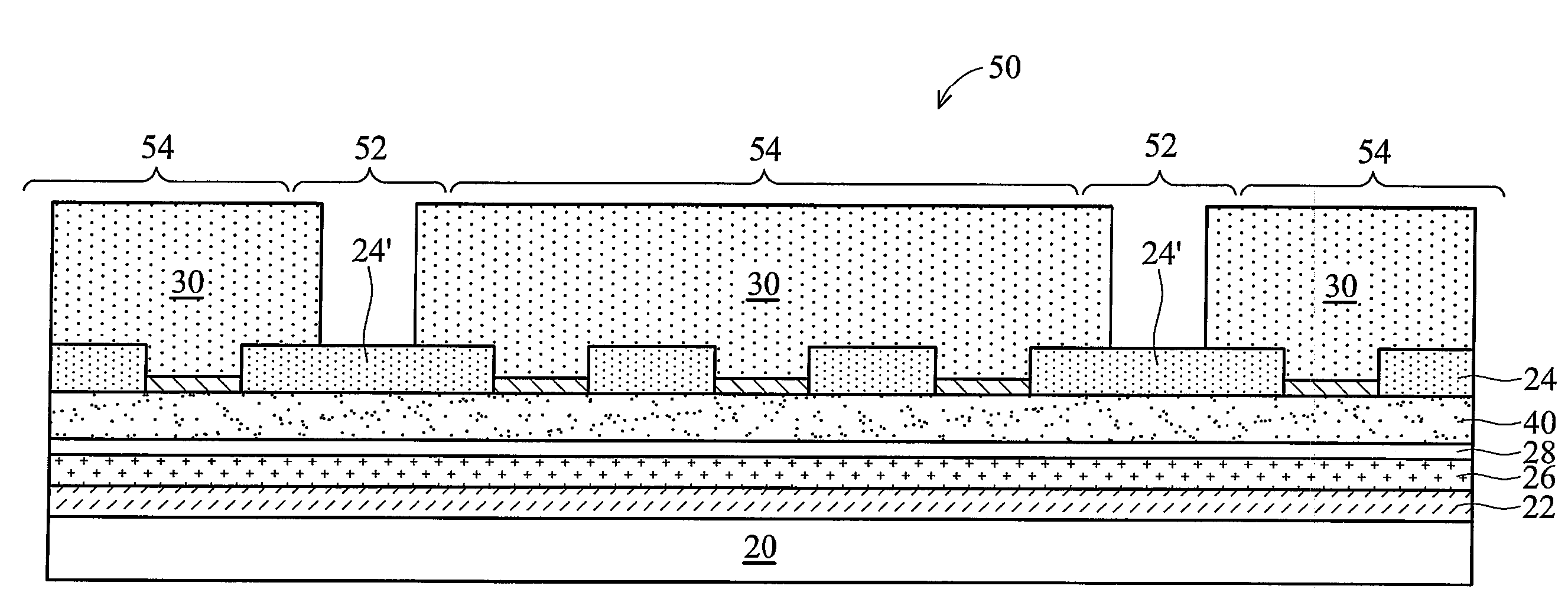
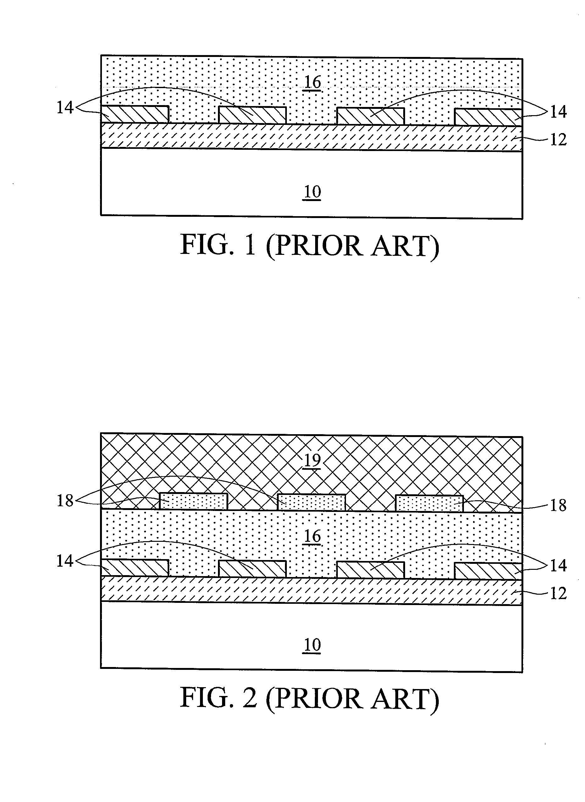
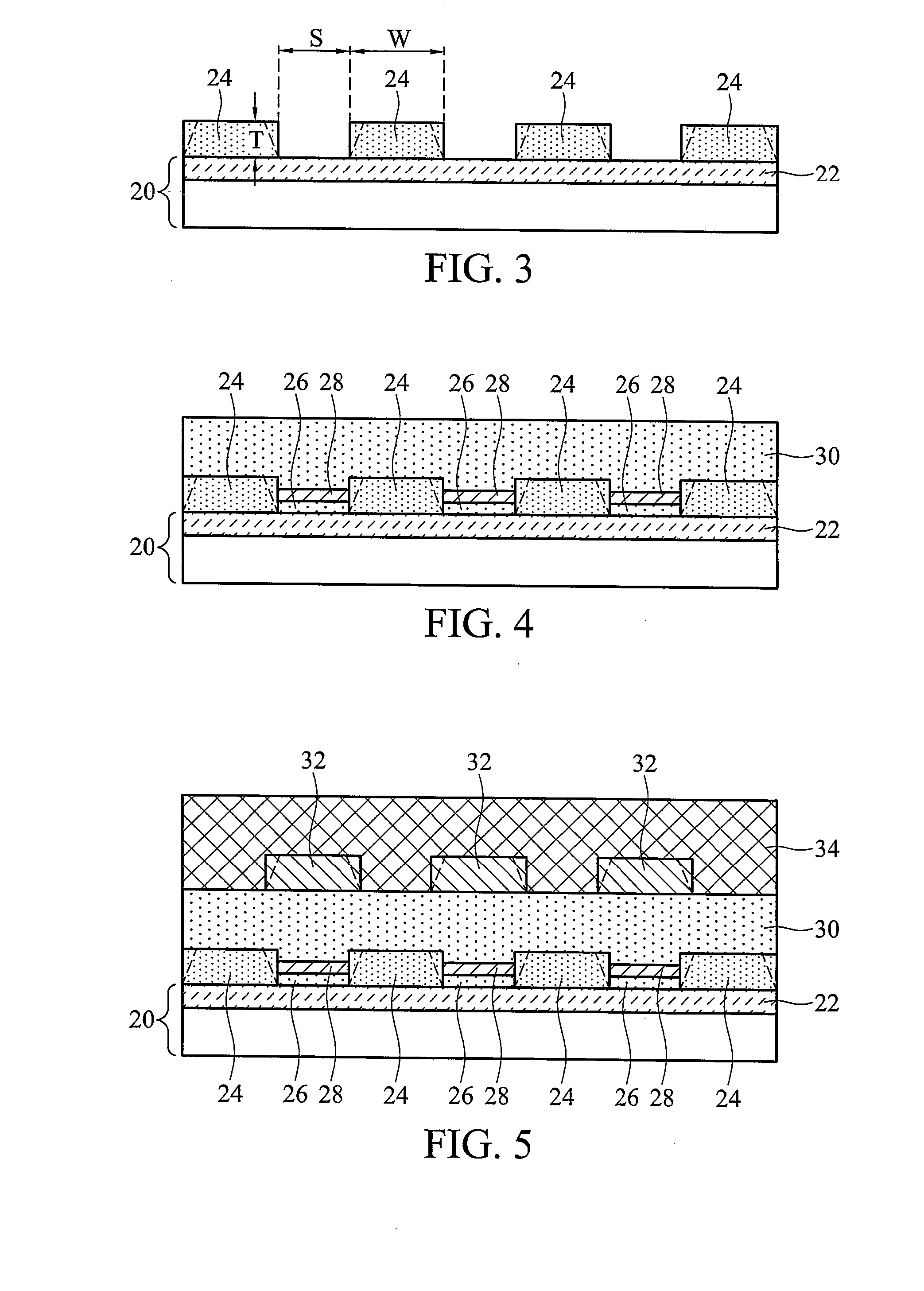
[0019]A novel method for forming group-III group-V (referred to as III-V hereinafter) semiconductor films and the resulting structures are provided. Throughout the description, the term “III-V compound semiconductor” refers to compound semiconductor materials comprising at least one group III element and one group-V element. The term “III-N compound semiconductor” refers to a III-V compound semiconductor in which the group V element is nitrogen. The required stages of manufacturing an illustrative embodiment of the present invention are illustrated. Those skilled in the art wi...


PUM


Abstract

A circuit structure includes a substrate; a patterned mask layer over the substrate, wherein the patterned mask layer includes a plurality of gaps; and a group-III group-V (III-V) compound semiconductor layer. The III-V compound semiconductor layer includes a first portion over the mask layer and second portions in the gaps, wherein the III-V compound semiconductor layer overlies a buffer / nucleation layer.

Description

[0001]This application claims the benefit of U.S. Provisional Application No. 61 / 087,921 filed on Aug. 11, 2008, entitled “III-V Compound Semiconductor Epitaxy Using Lateral Overgrowth,” which application is hereby incorporated herein by reference.TECHNICAL FIELD[0002]This invention relates generally to semiconductor circuit manufacturing processes and more particularly to forming group-III group-V (III-V) compound semiconductor films.BACKGROUND[0003]Group-III group-V compound semiconductors (often referred to as III-V compound semiconductors), such as gallium nitride (GaN) and its related alloys, have been under intense research in recent years due to their promising applications in electronic and optoelectronic devices. Particular examples of potential optoelectronic devices employing III-V compound semiconductors include blue light emitting diodes and laser diodes, and ultra-violet (UV) photo-detectors. The large band gap and high electron saturation velocity of many III-V compou...

Claims


Application Information

Patent Timeline
Patent Type & Authority Applications(United States)
IPC IPC(8): H01L29/20
CPCH01L21/0237H01L21/02458H01L21/02491H01L21/02502H01L21/0254H01L33/007H01L21/02645H01L21/8258H01L29/2003H01L29/66462H01L21/02642
Inventor YU, CHEN-HUAYU, CHIA-LINCHEN, DING-YUANCHIOU, WEN-CHIHLIN, HUNG-TA
Owner TAIWAN SEMICON MFG CO LTD
Why Eureka
Try Eureka