Display device and display drive method

a display device and drive technology, applied in the field of display devices and display drive methods, can solve the problems of difficult to realize large-sized and high-definition displays, and achieve the effect of improving the image quality of the display devi

Active Publication Date: 2010-02-25
JOLED INC
View PDF1 Cites 7 Cited by
  • Summary
  • Abstract
  • Description
  • Claims
  • Application Information

AI Technical Summary

Benefits of technology

[0006]As the pixel circuit configuration using the organic EL element, improvement of display quality as well as realization of high luminance, high definition and a high frame rate (high frequency) by eliminating luminance unevenness in each pixel and the like are strongly requested.
[0014]As the pixel circuit operation in the organic EL display device is performed in a higher frequency, the threshold correction operation of the drive transistor is performed in a time division manner in some cases. At this time, the drive transistor is cut off in the after-correction period, thereby suppressing the increase of the gate potential and the source potential to perform more accurate threshold correction.
[0016]According to another embodiment of the invention, when performing threshold correction in the time division manner, the drive transistor is cut off in the after-correction period, thereby performing threshold correction more suitably, and as a result, image quality of the display device can be improved. Additionally, as the method of cutting off the drive transistor, the intermediate voltage is supplied to the drive transistor and the coupling is formed through the parasitic capacitor between the gate and drain of the drive transistor, thereby performing cut-off control at high speed, which leads to the operation suitable also in a point of the operation in the higher frequency.

Problems solved by technology

The former has problems such that it is difficult to realize a large-sized as well as high-definition display though it has a simple configuration, therefore, the active-matrix type display device is vigorously developed at present.

Method used


Image

  • Display device and display drive method
  • Display device and display drive method
  • Display device and display drive method

Examples


Embodiment Construction

[0024]Hereinafter, as a display device according to an embodiment of the invention, an example of a display device using the organic EL element will be explained in the following order.[0025]1. Configuration of a display device according to an embodiment[0026]2. Pixel circuit operation in a process leading to an embodiment of the invention[0027]3. Pixel circuit operation as an embodiment of the invention

1. Configuration of a Display Device According to an Embodiment

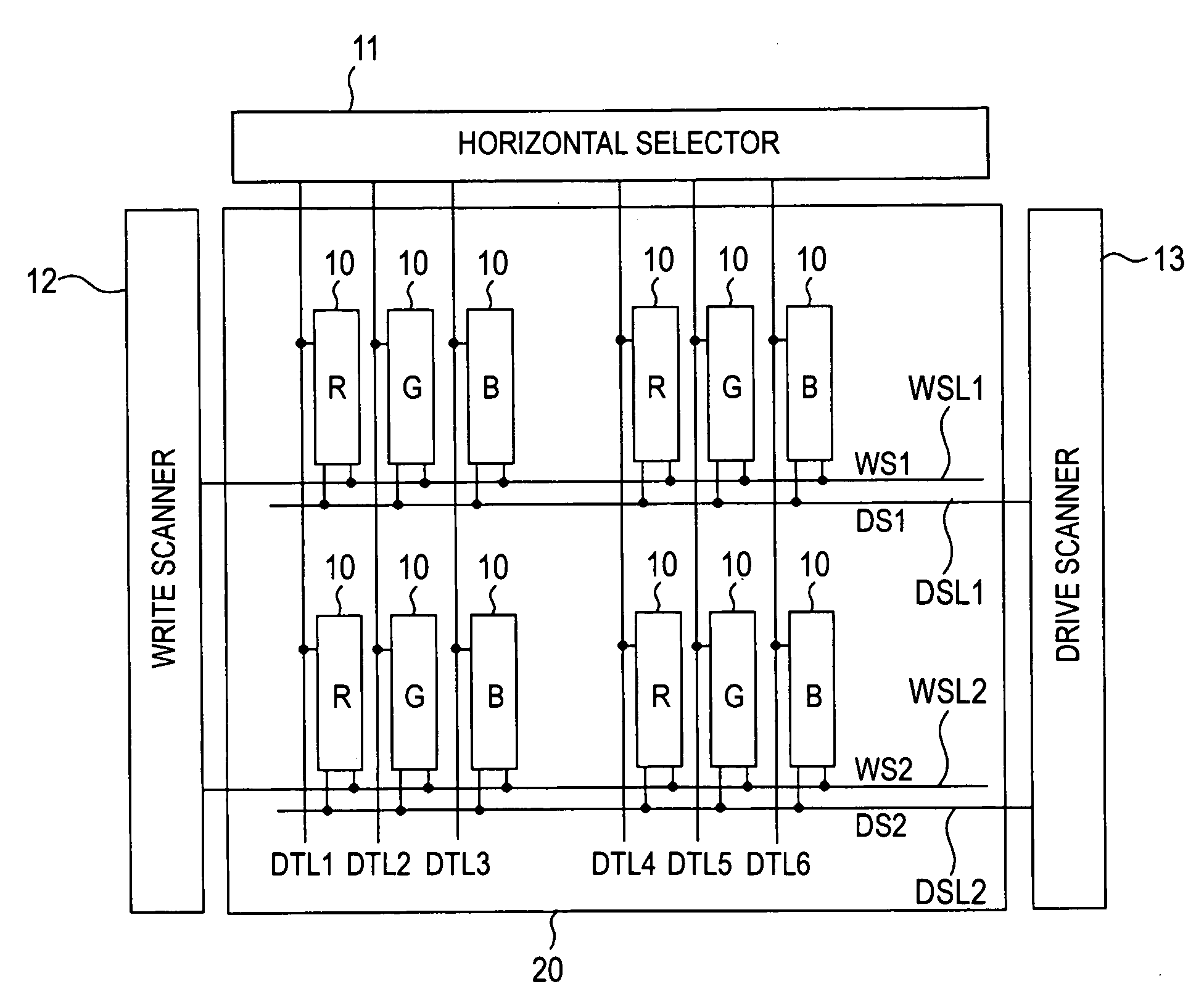
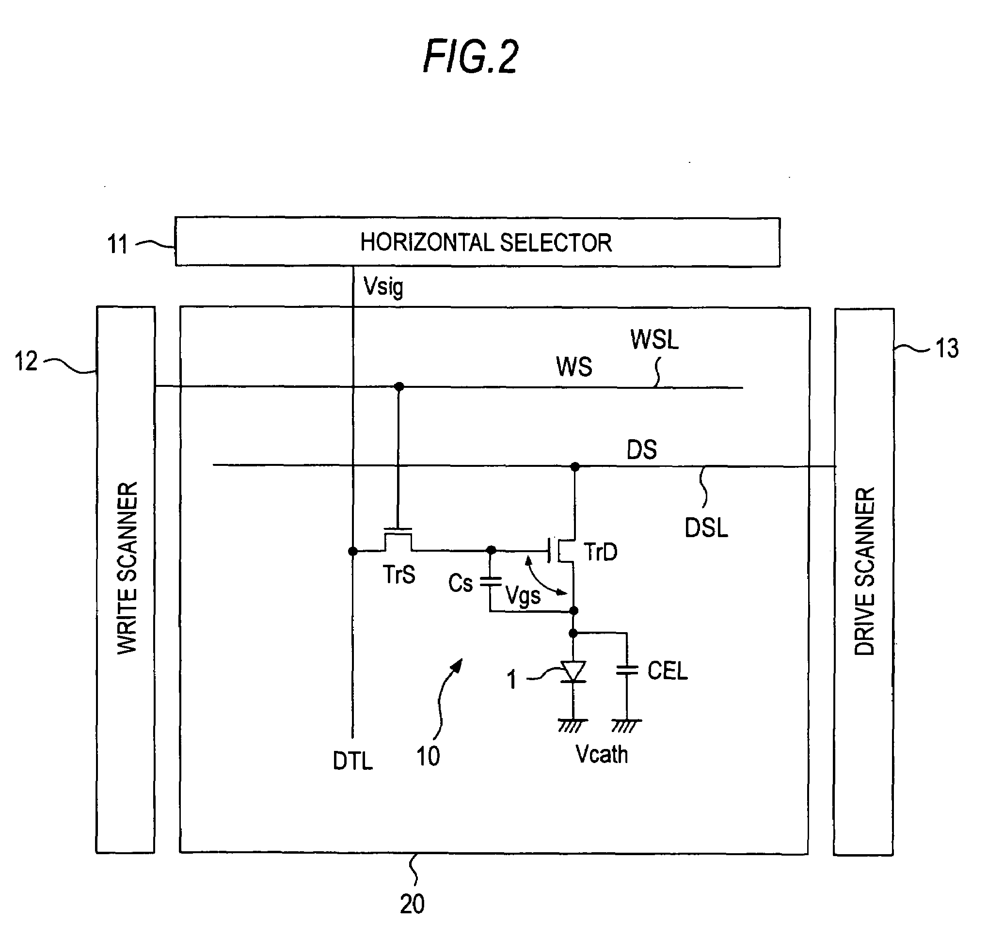
[0028]FIG. 1 shows the whole configuration of a display device according to an embodiment. The display device includes pixel circuits 10 having a correction function with respect to variation of a threshold voltage and mobility of a drive transistor as described later.

[0029]As shown in FIG. 1, the display device of the embodiment includes a pixel array unit 20 in which pixel circuits 10 are arranged in a column direction as well as in a row direction in a matrix state. “R”, “G” and “B” are given to the pixel circuits 10, ...


PUM


Abstract

A display device includes: a pixel array including pixel circuits arranged in a matrix state, in which each pixel circuit has a light emitting element, a drive transistor, and a storage capacitor storing a threshold voltage of the drive transistor and an inputted signal value; a threshold correction operation means for performing a threshold correction operation plural times, which allows the storage capacitor to store the threshold voltage of the drive transistor by supplying a drive voltage to the drive transistor in a state in which a gate potential of the drive transistor is in a reference value before giving the signal value to the storage capacitor; and a cut-off control means for cutting off the drive transistor by supplying an intermediate voltage which is lower than the drive voltage to the drive transistor in a after-correction period which is the period after the period of the threshold correction operation.

Description

BACKGROUND OF THE INVENTION[0001]1. Field of the Invention[0002]The invention relates to a display device including a pixel array in which pixel circuits are arranged in a matrix state and a display drive method thereof, and relates to, for example, a display device using an organic electroluminescence element (organic EL element) as a light emitting element.[0003]2. Description of the Related Art[0004]An image display device in which an organic EL element is used in a pixel is developed, for example as shown in JP-2003-255856 and JP-2003-271095 (Patent Documents 2 and 3). Since the organic EL element is a self-luminous element, it has advantages such that visibility of images is higher than, for example, a liquid crystal display, a backlight is not necessary and response speed is high. The luminance level (tone) of each light emitting element can be controlled by a value of current flowing therein (so-called current-control type).[0005]The organic EL display has a passive matrix ty...

Claims


Application Information

Patent Timeline
Patent Type & Authority Applications(United States)
IPC IPC(8): G09G5/00
CPCG09G3/3233G09G2300/0819G09G2320/043G09G2300/0861G09G2300/0842
Inventor YAMASHITA, JUNICHIUCHINO, KATSUHIDE
Owner JOLED INC
Why Eureka
Try Eureka