Fast wafer inspection system

a wafer inspection and wafer technology, applied in the direction of instruments, mass spectrometers, beam deviation/focusing by electric/magnetic means, etc., can solve the problem of limiting factors the response time of detectors

Active Publication Date: 2010-03-04
ICT INTEGRATED CIRCUIT TESTING GESELLSCHAFT FUER HALBLEITERPRUEFTECHNIK GMBH
View PDF11 Cites 20 Cited by
  • Summary
  • Abstract
  • Description
  • Claims
  • Application Information

AI Technical Summary

Problems solved by technology

Apart from sample change, beam calibration and beam scanning, o

Method used


Image

  • Fast wafer inspection system
  • Fast wafer inspection system
  • Fast wafer inspection system

Examples


Embodiment Construction

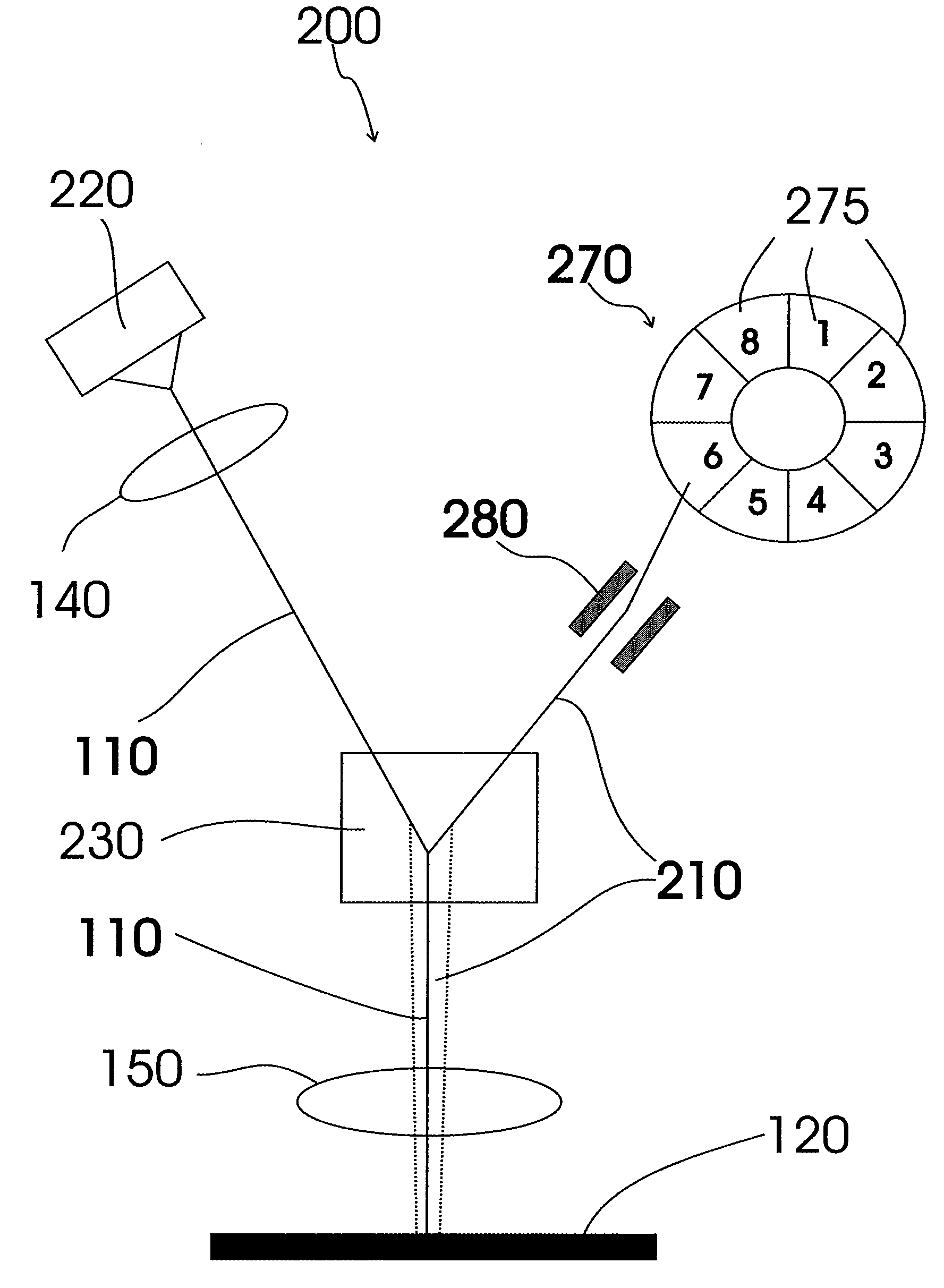
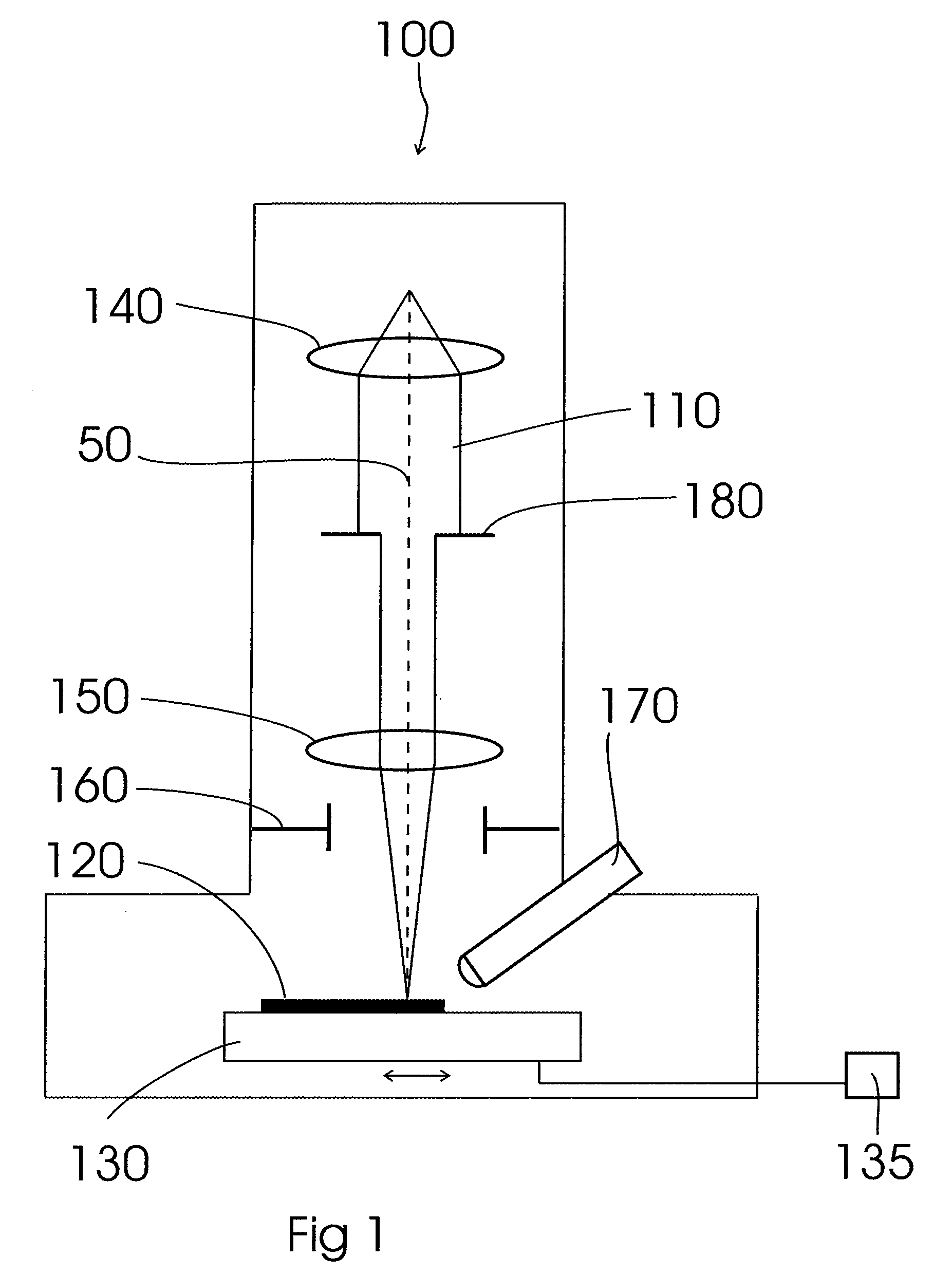
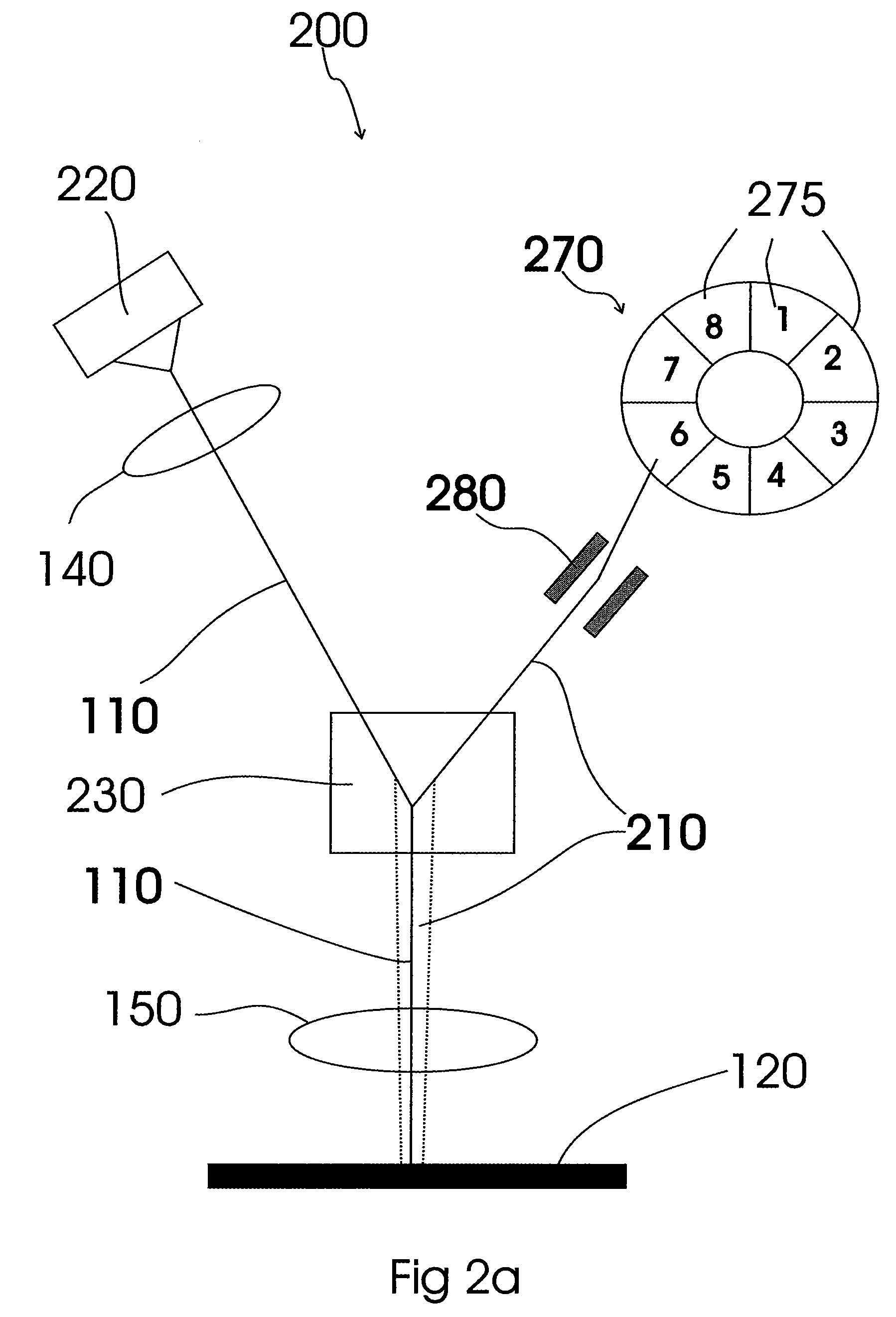
[0024]Reference will now be made in detail to the various embodiments of the invention, one or more examples of which are illustrated in the figures. Each example is provided by way of explanation of the invention and is not meant as a limitation of the invention. For example, features illustrated or described as part of one embodiment can be used on or in conjunction with other embodiments to yield yet a further embodiment. It is intended that the present invention includes such modifications and variations.

[0025]Without limiting the scope of protection of the present application, in the following description the charged particle beam device or components thereof will exemplarily be referred to as an electron beam device including the detection of secondary electrons. The present invention can still be applied for other charged particle apparatuses and / or for components detecting corpuscles such as secondary and / or backscattered charged particles in the form of electrons or ions, p...


PUM


Abstract

A charged particle beam device is provided including a particle source emitting a primary particle beam, a secondary particle beam generated by the impingement of the primary particle beam on the sample, a detection unit for detecting the secondary particle beam, the detector having at least two detector channels, and a distribution deflecting device for deflecting the secondary particle beam in a chronological sequence. Further, a detection assembly for a fast wafer inspection system is provided including a distribution deflecting device for distributing a secondary particle beam in a chronological sequence and a detector for detecting the secondary particle beam, the detector having multiple detector channels. Further, a method of operating a particle beam device with chronological resolution is provided.

Description

FIELD OF THE INVENTION[0001]The invention relates to a charged particle beam device and a method of operating a charged particle beam device. Particularly, it relates to a charged particle beam device having a particle source, in particular for imaging and / or inspecting a sample and a detector for detecting secondary particles. Further, it relates to a method of operating a particle beam device for high-speed inspection of a sample. Further, it relates to a detector assembly for a fast inspection system.BACKGROUND OF THE INVENTION[0002]Technologies such as microelectronics, micromechanics and biotechnology have created a high demand for structuring and probing specimens within the nanometer scale. Micrometer and nanometer scale process control, inspection or structuring, is often done with charged particle beams. Probing or structuring is often performed with charged particle beams which are generated and focused in charged particle beam devices. Examples of charged particle beam de...

Claims


Application Information

Patent Timeline
IPC IPC(8): G01N23/00H01J3/14
CPCH01J37/244H01J37/265H01J2237/24592H01J2237/24465H01J2237/24495H01J37/28
Inventor ADAMEC, PAVEL
Owner ICT INTEGRATED CIRCUIT TESTING GESELLSCHAFT FUER HALBLEITERPRUEFTECHNIK GMBH
Why Eureka
Try Eureka