
Liquid crystal display device

a display device and liquid crystal technology, applied in the field of liquid crystal display devices, can solve the problems of characteristic's viewing angle dependence problem, insufficient display performance, etc., and achieve the effect of higher transmittan

Inactive Publication Date: 2010-03-04
SHARP KK
View PDF9 Cites 19 Cited by
  • Summary
  • Abstract
  • Description
  • Claims
  • Application Information

AI Technical Summary

Benefits of technology

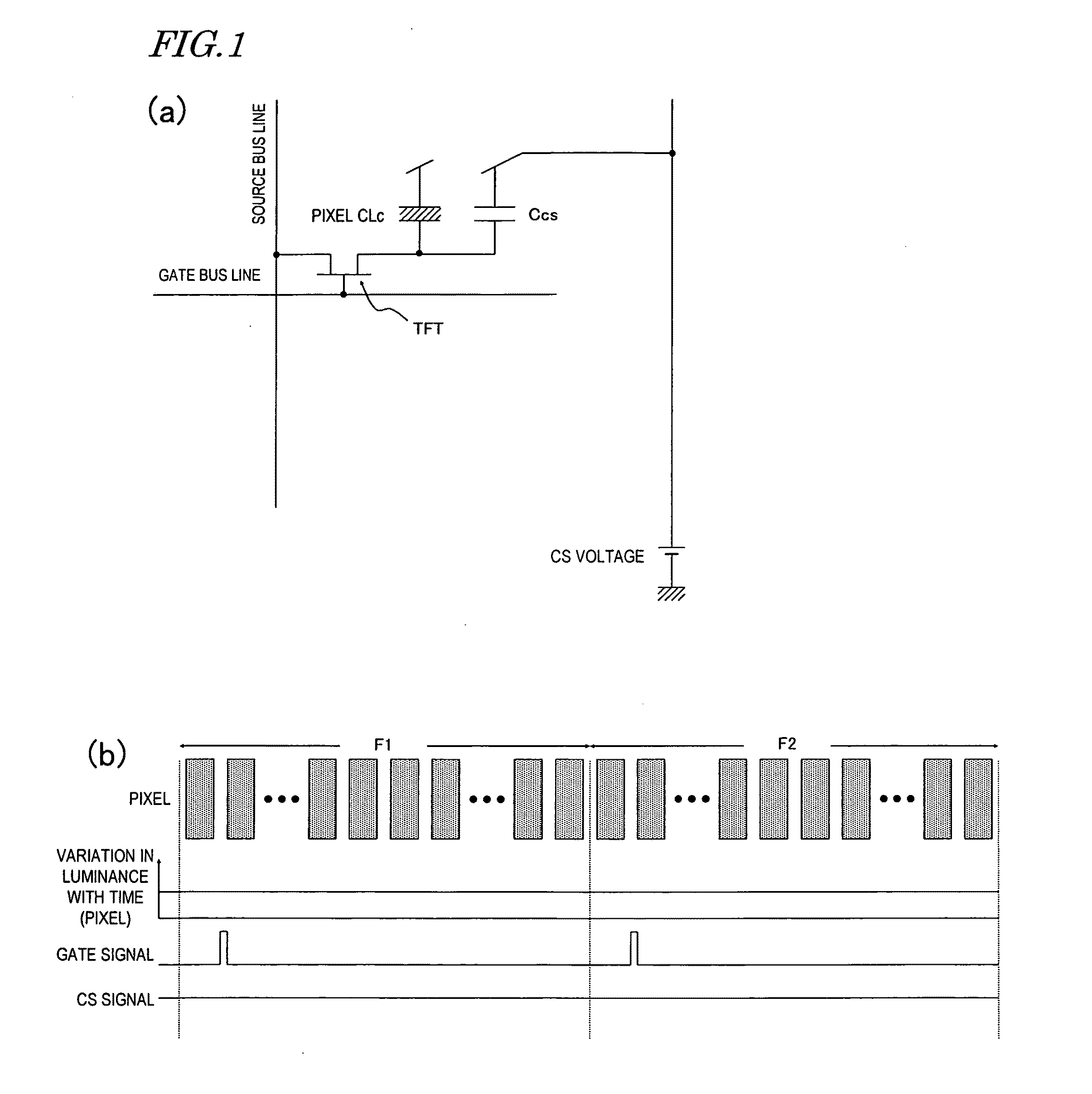
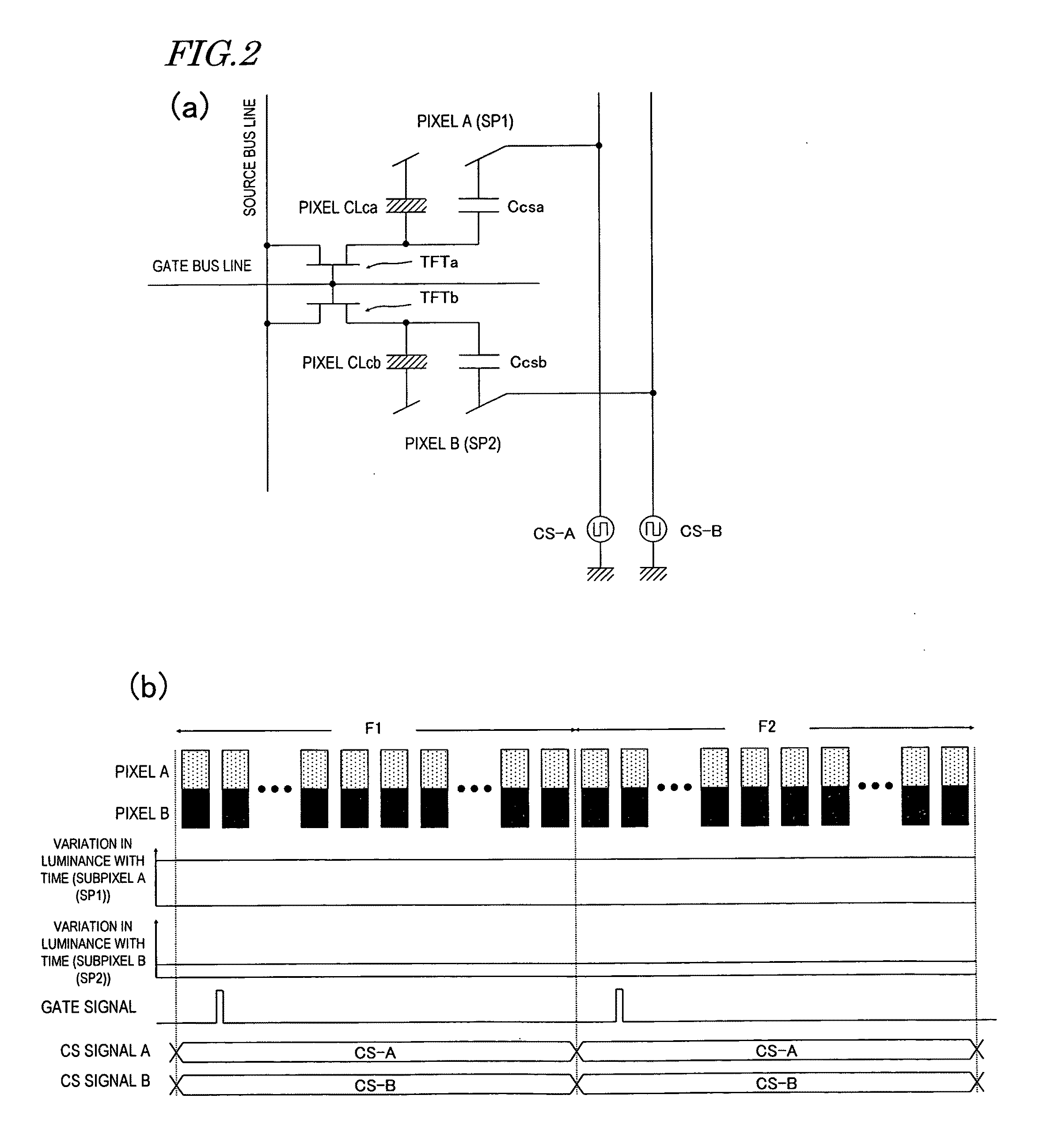
[0040]In the liquid crystal display device of the present invention, each pixel is divided not just spatially but also temporally. That is why compared to a conventional pixel division structure in which each pixel is divided only spatially, the liquid crystal display device of the present invention achieves a similar degree of viewing angle dependence of the γ characteristic and higher transmittance.

Problems solved by technology

However, the display performance (e.g., the viewing angle dependence of the γ characteristic, in particular) thereof is not fully satisfactory.
Although the display qualities of LCDs have been further improved nowadays, a γ characteristic's viewing angle dependence problem in a different phase has surfaced just recently.
This is a serious problem particularly when a still picture such as a photo is presented or when a TV program is displayed.
According to the IPS mode, however, it is more difficult to make panels that realize a high contrast ratio when the image on the screen is viewed straight with good productivity rather than in the MVA and ASM modes.

Method used


Image

  • Liquid crystal display device
  • Liquid crystal display device
  • Liquid crystal display device

Examples


embodiment 1

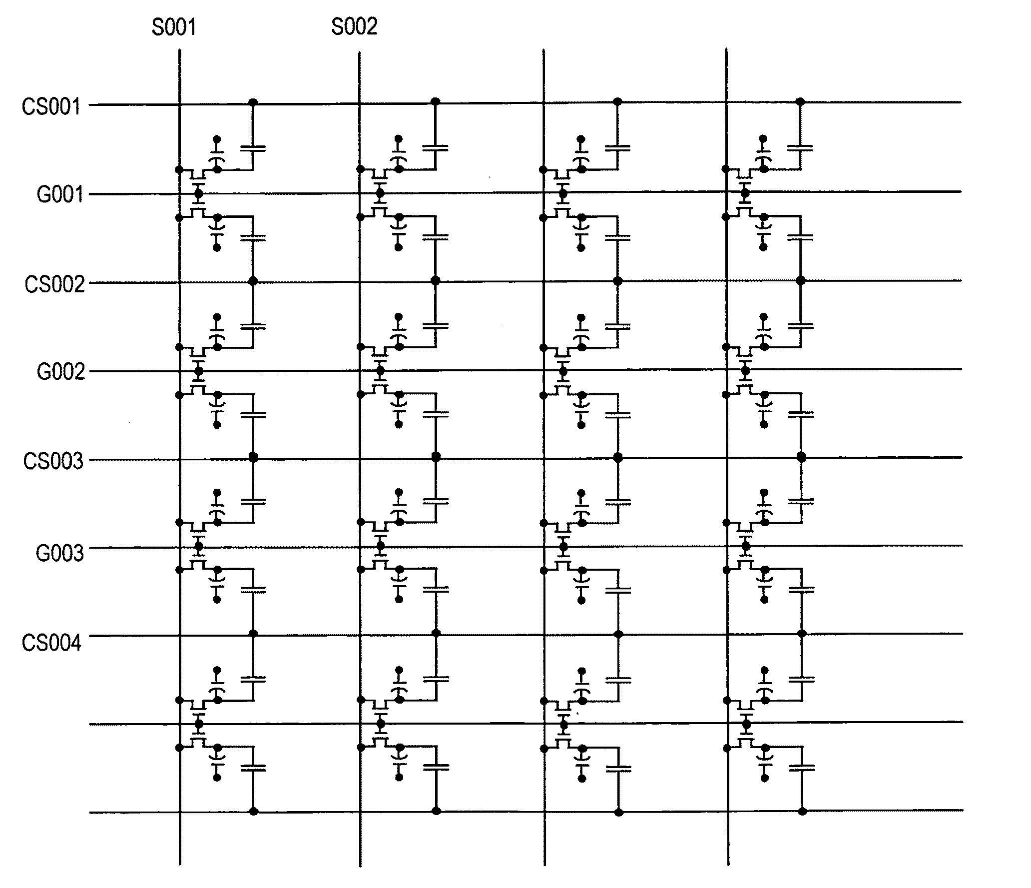
[0098]FIGS. 6a and 6b Illustrate the Waveforms of Cs Voltages applied to multi-pixel driven Inventive LCD 1 as a first preferred embodiment of the present invention and the effective voltages applied to subpixels. Inventive LCD 1 has the same pixel division structure as the one shown in FIG. 2(a) and also has the same connection pattern between CS bus lines and storage capacitors of respective subpixels as the one shown in FIG. 4C. FIGS. 6A and 6B respectively correspond to FIGS. 4A and 4B for Conventional LCD 2. That is to say, FIG. 6A illustrates waveforms for a bright subpixel and FIG. 6B illustrates waveforms for a dark subpixel.

[0099]Look how the CS voltage waveforms shown in FIGS. 6A and 6B change with time, and it can be seen that in an interval between a point in time when the gate voltage for an arbitrary pixel becomes VgH (to turn the TFT ON) and a point in time when the same voltage becomes VgH next time (to turn the TFT ON again), which corresponds to one vertical scanni...

embodiment 2

[0121]FIGS. 9A and 9B illustrate the waveforms of CS voltages applied to multi-pixel driven Inventive LCD 2 as a second preferred embodiment of the present invention and the effective voltages applied to subpixels. FIG. 9A illustrates waveforms for the bright subpixel, while FIG. 9B illustrates waveforms for the dark subpixel. And FIG. 9C illustrates how CS bus lines are connected to the respective storage capacitors of subpixels. In FIGS. 9A to 9C, the gate bus lines (corresponding to rows of pixels) are identified by l, m, o, q, r, s and t, which are integers that are equal to or greater than one and that represent the respective numbers of the gate bus lines. Naturally, these signs are totally different from the signs (including m and n) representing the division numbers as in FIGS. 4A to 4C.

[0122]In Inventive LCD 1 of the first preferred embodiment described above, in any of the bright and dark subpixels, both subpixels with positive and negative write polarities are controlled ...

embodiment 3

[0133]Patent Document No. 5 cited above discloses an example in which the number of electrically independent storage capacitor trunks (corresponding to the number of different CS voltages) is defined to be smaller than that of storage capacitor lines (i.e., CS bus lines). According to Patent Document No. 5, if each pixel is evenly split into two, the number of electrically independent storage capacitor trunks is defined to be smaller than twice the number of gate bus lines. However, the present invention is in no way limited to such a specific example. Instead, Inventive LCD 3 as a third preferred embodiment of the present invention adopts a configuration for supplying CS voltages to respective storage capacitor lines independently of each other. This Inventive LCD 3 has the advantage of increasing the number of options as first and second waveforms for the CS voltages. Nevertheless, each CS voltage should change its levels at least once after the gate voltage has gone low within on...


PUM


Abstract

In one embodiment of the present invention, a liquid crystal display device is disclosed, each pixel includes first and second subpixels, each of which includes a storage capacitor. Storage capacitor counter voltages applied independently to the storage capacitor counter electrodes of the first and second subpixels are varied within each vertical scanning period of the input video signal. As a result, each vertical scanning period of the input video signal includes a first subframe in which the first and second subpixels have luminances Y_SP1_A and Y_SP2_A, respectively, and a second subframe SFB in which the first and second subpixels have luminances Y_SP1_B and Y_SP2_B, respectively, where Y_SP1_A≠Y_SP2_A, Y_SP1_B≠Y_SP2_B, and Y_SP1_A≠Y_SP1_B or Y_SP2_A≠Y_SP2_B are satisfied. As a result, the viewing angle dependence of the γ characteristic can be reduced with the decrease in the transmittance of the liquid crystal display device minimized.

Description

TECHNICAL FIELD[0001]The present invention relates to a liquid crystal display device and a method for driving the device. More particularly, the present invention relates to a structure that can reduce the viewing angle dependence of the γ characteristic of a liquid crystal display device and a method for driving such a structure.BACKGROUND ART[0002]A liquid crystal display (LCD) is a flat-panel display that has a number of advantageous features including high resolution, drastically reduced thickness and weight, and low power dissipation. The LCD market has been rapidly expanding recently as a result of tremendous improvements in its display performance, significant increases in its productivity, and a noticeable rise in its cost effectiveness over competing technologies.[0003]A twisted-nematic (TN) mode liquid crystal display device, which used to be used extensively in the past, is subjected to an alignment treatment such that the major axes of its liquid crystal molecules, exhi...

Claims


Application Information

Patent Timeline
IPC IPC(8): G09G3/36G02F1/1343
CPCG02F1/136213G02F2001/134345G09G3/3607G09G2310/06G09G3/3655G09G2300/0443G09G2300/0447G09G3/3614G02F1/134345
Inventor SHIMOSHIKIRYOH, FUMIKAZU
Owner SHARP KK
Learn More